8-Bit
XC864
8-Bit Single-Chip Microcontroller
Data Sheet
V1.1 2009-03
Micr o co n t ro l l e rs
�Edition 2009-03
Published by
Infineon Technologies AG
81726 Munich, Germany
© 2009 Infineon Technologies AG
All Rights Reserved.
Legal Disclaimer
The information given in this document shall in no event be regarded as a guarantee of conditions or
characteristics. With respect to any examples or hints given herein, any typical values stated herein and/or any
information regarding the application of the device, Infineon Technologies hereby disclaims any and all warranties
and liabilities of any kind, including without limitation, warranties of non-infringement of intellectual property rights
of any third party.
Information
For further information on technology, delivery terms and conditions and prices, please contact the nearest
Infineon Technologies Office (www.infineon.com).
Warnings
Due to technical requirements, components may contain dangerous substances. For information on the types in
question, please contact the nearest Infineon Technologies Office.
Infineon Technologies components may be used in life-support devices or systems only with the express written
approval of Infineon Technologies, if a failure of such components can reasonably be expected to cause the failure
of that life-support device or system or to affect the safety or effectiveness of that device or system. Life support
devices or systems are intended to be implanted in the human body or to support and/or maintain and sustain
and/or protect human life. If they fail, it is reasonable to assume that the health of the user or other persons may
be endangered.
�8-Bit
XC864
8-Bit Single-Chip Microcontroller
Data Sheet
V1.1 2009-03
Micr o co n t ro l l e rs
�XC864 Data Sheet
Revision History:
2009-03
Previous Version:
V1.0
Page
V 1.1
Subjects (major changes since last revision)
Changes from V1.0 2008-08 to V1.1 2009-03
3
Modified the paragraph to remove the Automotive quality profile
We Listen to Your Comments
Any information within this document that you feel is wrong, unclear or missing at all?
Your feedback will help us to continuously improve the quality of this document.
Please send your proposal (including a reference to this document) to:
mcdocu.comments@infineon.com
�8-Bit Single-Chip Microcontroller
XC800 Family
1
XC864
Summary of Features
• High-performance XC800 Core
– compatible with standard 8051 processor
– two clocks per machine cycle architecture (for memory access without wait state)
– two data pointers
• On-chip memory
– 8 Kbytes of Boot ROM
– 256 bytes of RAM
– 512 bytes of XRAM
– 4 Kbytes of Flash for code (and data)
(includes memory protection strategy)
• I/O port supply at 3.3 V/5.0 V and core logic supply at 2.5 V (generated by embedded
voltage regulator)
(further features are on next page)
4K Bytes Flash
On-Chip Debug Support
Boot ROM
8K Bytes
UART
SSC
Port 0
6-bit Digital I/O
Capture/Compare Unit
16-bit
Port 1
1-bit Digital I/O
Compare Unit
16-bit
Port 2
4-bit Digital/Analog Input
Port 3
2-bit Digital I/O
XC800 Core
XRAM
512 Bytes
RAM
256 Bytes
Figure 1
Data Sheet
Timer 0
16-bit
Timer 1
16-bit
Timer 2
16-bit
Watchdog
Timer
ADC
10-bit
4-channel
XC864 Functional Units
1
V 1.1, 2009-03
�XC864
Summary of Features
Features (continued):
• Reset generation
– Power-On reset
– Hardware reset
– Brownout reset for core logic supply
– Watchdog timer reset
– Power-Down Wake-up reset
• On-chip OSC and PLL for clock generation
– PLL loss-of-lock detection
• Power saving modes
– slow-down mode
– idle mode
– power-down mode with wake-up capability via RXD or EXINT0
– clock gating control to each peripheral
• Programmable 16-bit Watchdog Timer (WDT)
• Four ports
– 9 pins as digital I/O
– 4 pins as digital/analog input
• 4-channel, 8-bit ADC
• Three 16-bit timers
– Timer 0 and Timer 1 (T0 and T1)
– Timer 2
• Capture/compare unit for PWM signal generation (CCU6)
• Full-duplex serial interface (UART)
• Synchronous serial channel (SSC)
• On-chip debug support
– 1 Kbyte of monitor ROM (part of the 8-Kbyte Boot ROM)
– 64 bytes of monitor RAM
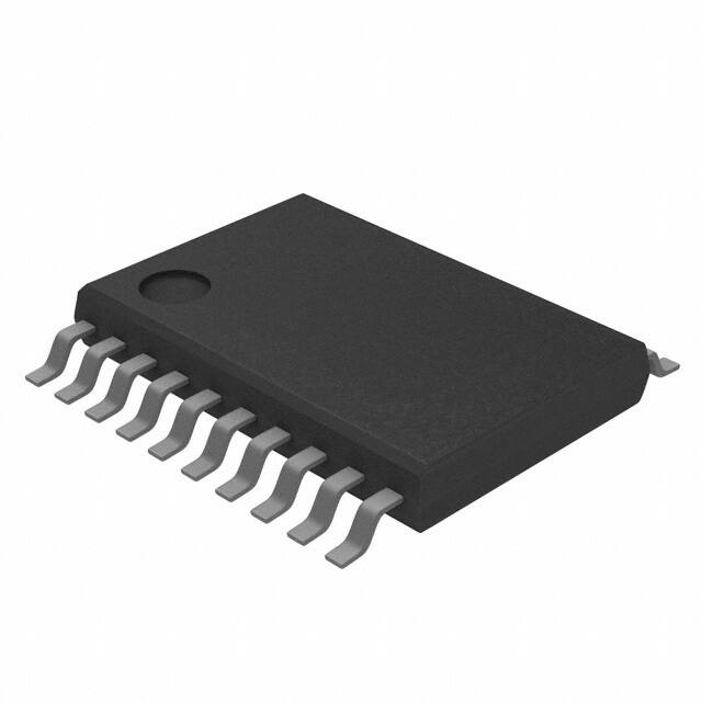
• PG-TSSOP-20 pin package
• Ambient temperature range TA:
– SAF (-40 to 85 °C)
– SAK (-40 to 125 °C)
Data Sheet
2
V 1.1, 2009-03
�XC864
Summary of Features
XC864 Variant Devices
The XC864 product family features devices with different power supply range and
temperature, offering cost-effective solution for different application requirements. The
package type available is TSSOP-20.
Table 1-1 summarizes the list of XC864 devices.
Table 1-1
Device Profile
Sales Type
Device Program
Type
Memory
(Kbytes)
Power TempQuality
Supply erature
Profile
(V)
Profile (°C)
SAK-XC864L-1FRI 5V
Flash
4
5.0
-40 to 125
Industrial
SAK-XC864L-1FRI 3V3
Flash
4
3.3
-40 to 125
Industrial
SAF-XC864L-1FRI 5V
Flash
4
5.0
-40 to 85
Industrial
SAF-XC864L-1FRI 3V3
Flash
4
3.3
-40 to 85
Industrial
Ordering Information
The ordering code for Infineon Technologies microcontrollers provides an exact
reference to the required product. This ordering code identifies:
• The derivative itself, i.e. its function set, the temperature range, and the supply voltage
• the package and the type of delivery
For the available ordering codes for the XC864, please refer to your responsible sales
representative or your local distributor.
As this document refers to all the derivatives, some descriptions may not apply to a
specific product. For simplicity all versions are referred to by the term XC864 throughout
this document.
Data Sheet
3
V 1.1, 2009-03
�XC864
General Device Information
2
General Device Information
2.1
Block Diagram
XC864
RESET
VDDP
VDDC
VSSC
T0 & T1
UART
P ort 0
TMS
256-byte RAM
+
64-byte monitor
RAM
P0.0 - P0.5
P ort 1
XC800 Core
P1.0/ P1.1
P ort 2
Internal Bus
8-Kbyte
Boot ROM 1)
P2.0 - P2.2, P2.7
CCU6
512-byte XRAM
SSC
4-Kbyte Flash
Timer 2
ADC
Clock Generator
OCDS
PLL
P ort 3
WDT
10 MHz
On-chip OSC
VAREF
VAGND/VSSP
P3.0 - P3.1
1) Includes 1-Kbyte monitor ROM
Figure 2
Data Sheet
XC864 Block Diagram
4
V 1.1, 2009-03
�XC864
General Device Information
2.2
Logic Symbol
VDDP
VSSP/VAGND
Port 0 6-Bit
VAREF
RESET
Port 1 1-Bit
TMS
XC864
Port 2 4-Bit
Port 3 2-Bit
VDDC
Figure 3
Data Sheet
VSSC
XC864 Logic Symbol
5
V 1.1, 2009-03
�XC864
General Device Information
2.3
Pin Configuration
The pin configuration of the XC864, which is based on the PG-TSSOP-20 package, is
shown in Figure 4. Every package pin is bonded to an input port pin or a bidirectional
port pin except Pin 15. It is bonded to 2 bidirectional port pins namely, P1.0 and P1.1.
Configurations of both port pins to output direction concurrently must be avoided to
prevent permanent damage to the chip1).
In addition, open drain output mode with pull-up device enabled is recommended for
P1.1 as TXD function and input mode for P1.0 as RXD function in single wire UART
communication.
P0.5/MRST_1/EXINT0_0/COUT62_1
1
20
P0.4/MTSR_1/CC62_1
VSSC
2
19
P0.3/SCK_1/COUT63_1
VDDC
3
18
RESET
TMS
4
17
P3.1/CCPOS0_2/CC61_2/COUT60_0
P0.0/TCK_0/T12HR_1/CC61_1/CLKOUT/RXDO_1
5
16
P0.2/CTRAP_2/TDO_0/TXD_1
6
P3.0/CC60_0/CCPOS1_2
P1.0/RXD_0/T2EX/
P1.1/EXINT3/TDO_1/TXD_0/T0
P0.1/TDI_0/T13HR_1/RXD_1/EXF2_1/COUT61_1
7
14
P2.7/AN7
P2.0/CCPOS0_0/EXINT1/T12HR_2/TCK_1/CC61_3/AN0
8
13
VAREF
P2.1/CCPOS1_0/EXINT2/T13HR_2/TDI_1/CC62_3/AN1
9
12
VAGND/VSSP
P2.2/CCPOS2_0/CTRAP_1/CC60_3/AN2
10
11
VDDP
Figure 4
1)
XC864
15
XC864 Pin Configuration, PG-TSSOP-20 Package (top view)
Protection against improper usage of P1.0 and P1.1 is not available in XC864.
Data Sheet
6
V 1.1, 2009-03
�XC864
General Device Information
2.4
Pin Definitions and Functions
Table 1
Pin Definitions and Functions
Symbol Pin
Type Reset Function
Number
State
P0
I/O
Port 0
Port 0 is an 8-bit bidirectional general purpose
I/O port. It can be used as alternate functions
for the JTAG, CCU6, UART, Timer 2 and SSC.
P0.0
5
Hi-Z
TCK_0
T12HR_1
P0.1
7
Hi-Z
TDI_0
T13HR_1
JTAG Clock Input
CCU6 Timer 12 Hardware Run
Input
CC61_1
Input/Output of Capture/
Compare channel 1
CLKOUT_0 Clock Output
RXDO_1
UART Transmit Data Output
RXD_1
COUT61_1
EXF2_1
JTAG Serial Data Input
CCU6 Timer 13 Hardware Run
Input
UART Receive Data Input
Output of Capture/Compare
channel 1
Timer 2 External Flag Output
P0.2
6
PU
CTRAP_2
TDO_0
TXD_1
CCU6 Trap Input
JTAG Serial Data Output
UART Transmit Data Output/
Clock Output
P0.3
19
Hi-Z
SCK_1
COUT63_1
SSC Clock Input/Output
Output of Capture/Compare
channel 3
P0.4
20
Hi-Z
MTSR_1
SSC Master Transmit Output/
Slave Receive Input
Input/Output of Capture/
Compare channel 2
CC62_1
P0.5
1
Hi-Z
MRST_1
EXINT0_0
COUT62_1
Data Sheet
7
SSC Master Receive Input/Slave
Transmit Output
External Interrupt Input 0
Output of Capture/Compare
channel 2
V 1.1, 2009-03
�XC864
General Device Information
Table 1
Pin Definitions and Functions (cont’d)
Symbol Pin
Type Reset Function
Number
State
P1
P1.0/
P1.1
I/O
15
Port 1
Port 1 is an 8-bit bidirectional general purpose
I/O port. It can be used as alternate functions
for the JTAG, CCU6, UART, Timer 0, Timer 2
and SSC.
PU
RXD_0
T2EX
EXINT3
T0
TDO_1
TXD_0
UART Receive Data Input
Timer 2 External Trigger Input
External Interrupt Input 3
Timer 0 Input
JTAG Serial Data Output
UART Transmit Data Output/
Clock Output
Note: Pin 15 is bonded to both P1.0 and P1.1
port pins. See Section 2.3 on the types
of port pin configuration to be avoided to
prevent permanent damage.
Data Sheet
8
V 1.1, 2009-03
�XC864
General Device Information
Table 1
Pin Definitions and Functions (cont’d)
Symbol Pin
Type Reset Function
Number
State
P2
I
Port 2
Port 2 is an 8-bit general purpose input-only
port. It can be used as alternate functions for
the digital inputs of the JTAG and CCU6. It is
also used as the analog inputs for the ADC.
P2.0
8
Hi-Z
CCPOS0_0 CCU6 Hall Input 0
EXINT1_0 External Interrupt Input 1
T12HR_2
CCU6 Timer 12 Hardware Run
Input
TCK_1
JTAG Clock Input
CC61_3
Input of Capture/Compare
channel 1
AN0
Analog Input 0
P2.1
9
Hi-Z
CCPOS1_0 CCU6 Hall Input 1
EXINT2_0 External Interrupt Input 2
T13HR_2
CCU6 Timer 13 Hardware Run
Input
TDI_1
JTAG Serial Data Input
CC62_3
Input of Capture/Compare
channel 2
AN1
Analog Input 1
P2.2
10
Hi-Z
CCPOS2_0 CCU6 Hall Input 2
CCU6 Trap Input
CTRAP_1
CC60_3
Input of Capture/Compare
channel 0
AN2
Analog Input 2
P2.7
14
Hi-Z
AN7
Data Sheet
Analog Input 7
9
V 1.1, 2009-03
�XC864
General Device Information
Table 1
Pin Definitions and Functions (cont’d)
Symbol Pin
Type Reset Function
Number
State
P3
I/O
Port 3
Port 3 is an 8-bit bidirectional general purpose
I/O port. It can be used as alternate functions
for CCU6.
P3.0
16
Hi-Z
CCPOS1_2 CCU6 Hall Input 1
CC60_0
Input/Output of Capture/
Compare channel 0
P3.1
17
Hi-Z
CCPOS0_2 CCU6 Hall Input 0
CC61_2
Input/Output of Capture/
Compare channel 1
COUT60_0 Output of Capture/Compare
channel 0
VDDP
11
–
–
I/O Port Supply (3.3 or 5.0 V)
Also used by EVR and analog modules. All
pins must be connected.
VDDC
VSSC
VAREF
VAGND/
VSSP
3
–
–
Core Supply Monitor (2.5 V)
2
–
–
Core Supply Ground
13
–
–
ADC Reference Voltage
12
–
–
ADC Reference Ground/
I/O Ground
All pins must be connected.
TMS
4
I
PD
Test Mode Select
I
PU
Reset Input
RESET 18
Data Sheet
10
V 1.1, 2009-03
�XC864
Functional Description
3
Functional Description
3.1
Processor Architecture
The XC864 is based on a high-performance 8-bit Central Processing Unit (CPU) that is
compatible with the standard 8051 processor. While the standard 8051 processor is
designed around a 12-clock machine cycle, the XC864 CPU uses a 2-clock machine
cycle. This allows fast access to ROM or RAM memories without wait state. Access to
the Flash memory, however, requires an additional wait state (one machine cycle). The
instruction set consists of 45% one-byte, 41% two-byte and 14% three-byte instructions.
The XC864 CPU provides a range of debugging features, including basic stop/start,
single-step execution, breakpoint support and read/write access to the data memory,
program memory and SFRs.
Figure 5 shows the CPU functional blocks.
Internal Data
Memory
Core SFRs
Register Interface
External Data
Memory
Program Memory
fCCLK
Memory Wait
Reset
Legacy External Interrupts (IEN0, IEN1)
External Interrupts
Non-Maskable Interrupt
Figure 5
Data Sheet
External SFRs
16-bit Registers &
Memory Interface
ALU
Opcode &
Immediate
Registers
Multiplier / Divider
Opcode Decoder
Timer 0 / Timer 1
State Machine &
Power Saving
UART
Interrupt
Controller
CPU Block Diagram
11
V 1.1, 2009-03
�XC864
Functional Description
3.2
Memory Organization
The XC864 consists of four types of memory:
• 8 Kbytes of Boot ROM program memory
• 256 bytes of internal RAM data memory
• 512 bytes of XRAM memory
(XRAM can be read/written as program memory or external data memory)
• 128 Special Function Register
• 4 Kbytes of Flash for code (and data)
Figure 6 illustrates the memory map of the address spaces of the XC864-1FR device.
FFFF H
XRAM
512 bytes
F200H
F000H
FFFF H
F200H
XRAM
512 bytes
F000H
E000H
Boot ROM
8 Kbytes
C000H
B000H
Flash
4 Kbytes
1)
A000H
3000H
Indirect
Address
2000H
Internal RAM
Direct
Address
FFH
Special Function
Registers
80H
1000H
7FH
Flash (overlayed )
4 Kbytes 1)
Internal RAM
0000H
Program Space
0000H
External Data Space
00H
Internal Data Space
1) For XC864 device, physically one 4KByte Flash bank is mapped to both address range 0000 H - 0FFFH and A000 H - AFFFH.
Figure 6
Data Sheet
Memory Map of XC864
12
V 1.1, 2009-03
�XC864
Functional Description
3.2.1
Memory Protection Strategy
The XC864 memory protection strategy includes:
• Read-out protection: The user is able to protect the contents in the Flash memory from
being read
• Flash program and erase protection: The Flash memory in all devices can be enabled
for program and erase protection
• Block external access and allow only boot in User Mode: Disable BSL and OCDS
modes.
Flash memory protection modes provided are:
• Mode 0: Protect against accidental erase and block external access.
• Mode 1: Read, program and erase protection are enabled, and block external access.
Flash protection is enabled by installing the user password via BSL mode 6. The user
setting of password for selection of each protection mode and the restrictions imposed
are summarized in Table 2. Flash protection mode 1 is meaningful only if the Flash is
used for code only. Otherwise if the Flash is used partially for code and partially for data,
then only Flash protection mode 0 is meaningful.
Note: In XC864, the type of Flash protection scheme will affect the entering of BSL Mode
once User Mode is entered.
Table 2
Flash Protection Modes
Mode
0
1
Selection
MSB of password = 0
MSB of password = 1
Flash contents
can be read by
Read instructions in any program
memory
Read instructions in Flash
Flash program
Possible
Not possible
Data Sheet
13
V 1.1, 2009-03
�XC864
Functional Description
Table 2
Flash Protection Modes (cont’d)
Flash erase
Possible, on condition that bit
DFLASHEN in register MISC_CON
is set to 1 prior to each erase
operation
Not possible
Additional
Protection
Block external access (can only start Block external access (can
in User Mode)
only start in User Mode)
Possible; For detailed
Subsequent
Possible1); For detailed
descriptions, see “User Mode Entry descriptions, see “User
entering of BSL
Mode Entry 2” on Page 59
mode with LSB of 2” on Page 59
password is 1
Not possible1)
|Subsequent
entering of BSL
mode with LSB of
password is 0
1)
Not possible
With MSB of password = 0, Flash content can be upgraded using a predefined routine in the user code via InApplication Programming(IAP). Programming via BSL mode is not needed. See “User Mode Entry 3” on
Page 60.
BSL mode 6, which is used for enabling Flash protection, can also be used for disabling
Flash protection. Here, the programmed password must be provided by the user. A
password match triggers an automatic erase of the read-protected Flash contents
(sector(s) to erase is defined by password, see Table 3), and the programmed password
is erased. The Flash protection is then disabled upon the next reset.
Data Sheet
14
V 1.1, 2009-03
�XC864
Functional Description
Table 3
Password Definition
Password
To Enable Protection:
Type of Hardware
Protection1)
To Remove Protection:
Sectors to Erase2) before Remove
Hardware Protection
1XXXXXXXB
Read/Program/Erase
All Sectors
00001XXXB
Erase
Sector 0
00010XXXB
Erase
Sector 0 and 1
00011XXXB
Erase
Sector 0 to 2
00100XXXB
Erase
Sector 0 to 3
00101XXXB
Erase
Sector 0 to 4
00110XXXB
Erase
Sector 0 to 5
00111XXXB
Erase
Sector 0 to 6
01000XXXB
Erase
Sector 0 to 7
01001XXXB
Erase
Sector 0 to 8
01010XXXB
Erase
All Sector
Others
Erase
None
1)
On the whole Flash. This hardware protection is complimented by the ‘block external access’ feature (see
Table 2).
2)
Controlled automatically by BSL mode 6 routine in Boot ROM, based on the password previously installed by
the user when enabling Flash protection.
Although no protection scheme can be considered infallible, the XC864 memory
protection strategy provides a very high level of protection for a general purpose
microcontroller.
Data Sheet
15
V 1.1, 2009-03
�XC864
Functional Description
3.2.2
Special Function Register
The Special Function Registers (SFRs) occupy direct internal data memory space in the
range 80H to FFH. All registers, except the program counter, reside in the SFR area. The
SFRs include pointers and registers that provide an interface between the CPU and the
on-chip peripherals. As the 128-SFR range is less than the total number of registers
required, address extension mechanisms are required to increase the number of
addressable SFRs. The address extension mechanisms include:
• Mapping
• Paging
3.2.2.1
Address Extension by Mapping
Address extension is performed at the system level by mapping. The SFR area is
extended into two portions: the standard (non-mapped) SFR area and the mapped SFR
area. Each portion supports the same address range 80H to FFH, bringing the number
of addressable SFRs to 256. The extended address range is not directly controlled by
the CPU instruction itself, but is derived from bit RMAP in the system control register
SYSCON0 at address 8FH. To access SFRs in the mapped area, bit RMAP in SFR
SYSCON0 must be set. Alternatively, the SFRs in the standard area can be accessed
by clearing bit RMAP. The SFR area can be selected as shown in Figure 7.
SYSCON0
System Control Register 0
7
6
Reset Value: 04H
5
4
3
2
1
0
0
1
0
RMAP
r
rw
r
rw
Field
Bits
Type Description
RMAP
0
rw
Special Function Register Map Control
0
The access to the standard SFR area is
enabled.
1
The access to the mapped SFR area is
enabled.
1
2
rw
Reserved
Returns the last value if read; should be written
with 1.
0
1,[7:3]
r
Reserved
Returns 0 if read; should be written with 0.
Data Sheet
16
V 1.1, 2009-03
�XC864
Functional Description
Note: The RMAP bit must be cleared/set by ANL or ORL instructions.
As long as bit RMAP is set, the mapped SFR area can be accessed. This bit is not
cleared automatically by hardware. Thus, before standard/mapped registers are
accessed, bit RMAP must be cleared/set, respectively, by software.
Standard Area (RMAP = 0)
FFH
Module 1 SFRs
Module 2 SFRs
SYSCON0.RMAP
rw
…...
Module n SFRs
80 H
SFR Data
(to/from CPU)
Mapped Area (RMAP = 1)
FFH
Module (n+1) SFRs
Module (n+2) SFRs
…...
Module m SFRs
80 H
Direct
Internal Data
Memory Address
Figure 7
Data Sheet
Address Extension by Mapping
17
V 1.1, 2009-03
�XC864
Functional Description
3.2.2.2
Address Extension by Paging
Address extension is further performed at the module level by paging. With the address
extension by mapping, the XC864 has a 256-SFR address range. However, this is still
less than the total number of SFRs needed by the on-chip peripherals. To meet this
requirement, some peripherals have a built-in local address extension mechanism for
increasing the number of addressable SFRs. The extended address range is not directly
controlled by the CPU instruction itself, but is derived from bit field PAGE in the module
page register MOD_PAGE. Hence, the bit field PAGE must be programmed before
accessing the SFR of the target module. Each module may contain a different number
of pages and a different number of SFRs per page, depending on the specific
requirement. Besides setting the correct RMAP bit value to select the SFR area, the user
must also ensure that a valid PAGE is selected to target the desired SFR. A page inside
the extended address range can be selected as shown in Figure 8.
SFR Address
(from CPU)
PAGE 0
MOD_PAGE.PAGE
SFR0
rw
SFR1
…...
SFRx
PAGE 1
SFR0
SFR Data
(to/from CPU)
SFR1
…...
SFRy
…...
PAGE q
SFR0
SFR1
…...
SFRz
Module
Figure 8
Data Sheet
Address Extension by Paging
18
V 1.1, 2009-03
�XC864
Functional Description
In order to access a register located in a page different from the actual one, the current
page must be left. This is done by reprogramming the bit field PAGE in the page register.
Only then can the desired access be performed.
If an interrupt routine is initiated between the page register access and the module
register access, and the interrupt needs to access a register located in another page, the
current page setting can be saved, the new one programmed and finally, the old page
setting restored. This is possible with the storage fields STx (x = 0 - 3) for the save and
restore action of the current page setting. By indicating which storage bit field should be
used in parallel with the new page value, a single write operation can:
• Save the contents of PAGE in STx before overwriting with the new value
(this is done in the beginning of the interrupt routine to save the current page setting
and program the new page number); or
• Overwrite the contents of PAGE with the contents of STx, ignoring the value written to
the bit positions of PAGE
(this is done at the end of the interrupt routine to restore the previous page setting
before the interrupt occurred)
ST3
ST2
ST1
ST0
STNR
PAGE
value update
from CPU
Figure 9
Storage Elements for Paging
With this mechanism, a certain number of interrupt routines (or other routines) can
perform page changes without reading and storing the previously used page information.
The use of only write operations makes the system simpler and faster. Consequently,
this mechanism significantly improves the performance of short interrupt routines.
The XC864 supports local address extension for:
•
•
•
•
Parallel Ports
Analog-to-Digital Converter (ADC)
Capture/Compare Unit 6 (CCU6)
System Control Registers
The page register has the following definition:
Data Sheet
19
V 1.1, 2009-03
�XC864
Functional Description
MOD_PAGE
Page Register for module MOD
7
6
Reset Value: 00H
5
4
3
2
1
OP
STNR
0
PAGE
w
w
r
rwh
0
Field
Bits
Type Description
PAGE
[2:0]
rwh
Page Bits
When written, the value indicates the new page.
When read, the value indicates the currently active
page.
STNR
[5:4]
w
Storage Number
This number indicates which storage bit field is the
target of the operation defined by bit field OP.
If OP = 10B,
the contents of PAGE are saved in STx before being
overwritten with the new value.
If OP = 11B,
the contents of PAGE are overwritten by the
contents of STx. The value written to the bit positions
of PAGE is ignored.
00
ST0 is selected.
01
ST1 is selected.
10
ST2 is selected.
11 ST3 is selected.
OP
[7:6]
w
Operation
0X Manual page mode. The value of STNR is
ignored and PAGE is directly written.
10
New page programming with automatic page
saving. The value written to the bit positions of
PAGE is stored. In parallel, the previous
contents of PAGE are saved in the storage bit
field STx indicated by STNR.
11
Automatic restore page action. The value
written to the bit positions PAGE is ignored
and instead, PAGE is overwritten by the
contents of the storage bit field STx indicated
by STNR.
Data Sheet
20
V 1.1, 2009-03
�XC864
Functional Description
Field
Bits
Type Description
0
3
r
Data Sheet
Reserved
Returns 0 if read; should be written with 0.
21
V 1.1, 2009-03
�XC864
Functional Description
3.2.3
Bit Protection Scheme
The bit protection scheme prevents direct software writing of selected bits (i.e., protected
bits) using the PASSWD register. When the bit field MODE is 11B, writing 10011B to the
bit field PASS opens access to writing of all protected bits, and writing 10101B to the bit
field PASS closes access to writing of all protected bits. Note that access is opened for
maximum 32 CCLKs if the “close access” password is not written. If “open access”
password is written again before the end of 32 CCLK cycles, there will be a recount of
32 CCLK cycles. The protected bits include NDIV, WDTEN, PD, and SD.
PASSWD
Password Register
7
Reset Value: 07H
6
5
4
3
2
1
0
PASS
PROTECT
_S
MODE
w
rh
rw
Field
Bits
Type Description
MODE
[1:0]
rw
Bit Protection Scheme Control bits
00
Scheme Disabled
11
Scheme Enabled (default)
Others: Scheme Enabled
These two bits cannot be written directly. To change
the value between 11B and 00B, the bit field PASS
must be written with 11000B; only then, will the
MODE[1:0] be registered.
PROTECT_S
2
rh
Bit Protection Signal Status bit
This bit shows the status of the protection.
0
Software is able to write to all protected bits.
1
Software is unable to write to any protected
bits.
PASS
[7:3]
w
Password bits
The Bit Protection Scheme only recognizes three
patterns.
11000B Enables writing of the bit field MODE.
10011B Opens access to writing of all protected bits.
10101B Closes access to writing of all protected bits.
Data Sheet
22
V 1.1, 2009-03
�XC864
Functional Description
3.2.4
XC864 Register Overview
The SFRs of the XC864 are organized into groups according to their functional units. The
contents (bits) of the SFRs are summarized in Table 4 to Table 12, with the addresses
of the bitaddressable SFRs appearing in bold typeface.
Note: Bits marked as 0 or 1 must be initialized per se, the functionality of the device with
the other setting is not guaranteed.
The CPU SFRs can be accessed in both the standard and mapped memory areas
(RMAP = 0 or 1).
Table 4
Addr
CPU Register Overview
Register Name
RMAP = 0 or 1
SP
81H
Stack Pointer Register
Bit
Reset: 07H
Bit Field
Type
82H
DPL
Reset: 00H
Data Pointer Register Low
Bit Field
Type
83H
DPH
Reset: 00H
Data Pointer Register High
Bit Field
Type
87H
PCON
Power Control Register
Reset: 00H
Bit Field
Type
88H
TCON
Timer Control Register
Reset: 00H
Bit Field
Type
89H
TMOD
Timer Mode Register
Reset: 00H
Bit Field
Type
8AH
TL0
Timer 0 Register Low
Reset: 00H
Bit Field
Type
8BH
TL1
Timer 1 Register Low
Reset: 00H
Bit Field
Type
8CH
TH0
Timer 0 Register High
Reset: 00H
Bit Field
Type
8DH
TH1
Timer 1 Register High
Reset: 00H
Bit Field
Type
98H
SCON
Reset: 00H
Serial Channel Control Register
Bit Field
Type
99H
SBUF
Reset: 00H
Serial Data Buffer Register
Bit Field
Type
A2H
EO
Reset: 00H
Extended Operation Register
Bit Field
A8H
IEN0
Reset: 00H
Interrupt Enable Register 0
Bit Field
Type
B8H
IP
Reset: 00H
Interrupt Priority Register
Bit Field
Type
B9H
IPH
Reset: 00H
Interrupt Priority Register High
Bit Field
Type
D0H
PSW
Reset: 00H
Program Status Word Register
Bit Field
Type
7
6
DPL7 DPL6
rw
rw
DPH7 DPH6
rw
rw
SMOD
rw
TF1
TR1
rwh
rw
GATE1
0
rw
r
SM0
rw
SM1
rw
SM2
rw
0
r
0
r
0
r
CY
rwh
23
AC
rwh
3
VAL
rwh
REN
TB8
rw
rw
VAL
rwh
TRAP_
EN
rw
r
EA
rw
4
2
1
SP
rw
DPL5 DPL4 DPL3 DPL2
rw
rw
rw
rw
DPH5 DPH4 DPH3 DPH2
rw
rw
rw
rw
0
GF1
GF0
r
rw
rw
TF0
TR0
IE1
IT1
rwh
rw
rwh
rw
T1M
GATE0 T0S
rw
rw
rw
VAL
rwh
VAL
rwh
VAL
rwh
0
Type
Data Sheet
5
ET2
rw
PT2
rw
PT2H
rw
F0
rw
ES
rw
PS
rw
PSH
rw
RS1
rw
ET1
rw
PT1
rw
PT1H
rw
RS0
rw
RB8
rwh
0
DPL1 DPL0
rw
rw
DPH1 DPH0
rw
rw
0
IDLE
r
rw
IE0
IT0
rwh
rw
T0M
rw
TI
rwh
0
RI
rwh
DPSEL
0
rw
r
EX1
rw
PX1
rw
PX1H
rw
OV
rwh
ET0
rw
PT0
rw
PT0H
rw
F1
rw
EX0
rw
PX0
rw
PX0H
rw
P
rh
V 1.1, 2009-03
�XC864
Functional Description
Table 4
CPU Register Overview (cont’d)
Addr
Register Name
E0H
ACC
Accumulator Register
Bit
E8H
IEN1
Reset: 00H
Interrupt Enable Register 1
F0H
B
B Register
F8H
IP1
Reset: 00H
Interrupt Priority Register 1
F9H
IPH1
Reset: 00H
Interrupt Priority Register 1 High
Reset: 00H
Reset: 00H
Bit Field
Type
Bit Field
Type
Bit Field
Type
Bit Field
Type
Bit Field
Type
2
1
0
ACC7 ACC6 ACC5 ACC4 ACC3
rw
rw
rw
rw
rw
ECCIP ECCIP ECCIP ECCIP EXM
3
2
1
0
rw
rw
rw
rw
rw
B7
B6
B5
B4
B3
rw
rw
rw
rw
rw
PCCIP PCCIP PCCIP PCCIP PXM
3
2
1
0
rw
rw
rw
rw
rw
7
6
5
4
3
ACC2
rw
EX2
ACC1
rw
ESSC
ACC0
rw
EADC
rw
B2
rw
PX2
rw
B1
rw
PSSC
rw
B0
rw
PADC
rw
rw
rw
PCCIP PCCIP PCCIP PCCIP PXMH
3H
2H
1H
0H
rw
rw
rw
rw
rw
PX2H PSSCH PADC
H
rw
rw
rw
The system control SFRs can be accessed in the standard memory area (RMAP = 0). A
special case is SYSCON0 which can be accessed in both the standard and mapped
memory areas (RMAP = 0 or 1).
Table 5
Addr
SCU Register Summary
Register Name
Bit
7
6
5
4
RMAP = 0 or 1
SYSCON0
Reset: 04H
8FH
System Control Register 0
Bit Field
Type
RMAP = 0
SCU_PAGE
BFH
Page Register
Bit Field
Type
OP
w
STNR
w
Bit Field
0
Type
r
JTAGT JTAGT
DIS
CKS
rw
rw
Reset: 00H
RMAP = 0, PAGE 0
MODPISEL
Reset: 00H
B3H
Peripheral Input Select Register
B4H
IRCON0
Reset: 00H
Interrupt Request Register 0
B5H
IRCON1
Reset: 00H
Interrupt Request Register 1
B7H
EXICON0
Reset: 00H
External Interrupt Control Register 0
BBH
NMICON
NMI Control Register
Reset: 00H
BCH
NMISR
NMI Status Register
Reset: 00H
BDH
BCON
Reset: 00H
Baud Rate Control Register
Bit Field
Type
BEH
BG
Reset: 00H
Baud Rate Timer/Reload Register
Bit Field
Type
Data Sheet
0
r
0
Bit Field
Type
Bit Field
Type
Bit Field
Type
r
0
Type
r
EXINT3
rw
0
NMI
ECC
r
rw
Bit Field
0
Type
r
Bit Field
3
FNMI
ECC
rwh
BGSEL
rw
24
2
1
0
1
rw
0
r
RMAP
rw
0
r
PAGE
rwh
0
EXINT URRIS
0IS
r
rw
rw
EXINT EXINT EXINT EXINT
3
2
1
0
rwh
rwh
rwh
rwh
ADCS ADCS
RIR
TIR
EIR
RC1
RC0
rwh
rwh
rwh
rwh
rwh
EXINT2
EXINT1
EXINT0
rw
rw
rw
NMI
NMI
NMI
NMI
NMI
NMI
VDDP VDD OCDS FLASH PLL
WDT
rw
rw
rw
rw
rw
rw
FNMI FNMI FNMI FNMI FNMI FNMI
VDDP VDD OCDS FLASH PLL
WDT
rwh
rwh
rwh
rwh
rwh
rwh
0
r
BRDIS
rw
BR_VALUE
rwh
BRPRE
rw
R
rw
V 1.1, 2009-03
�XC864
Functional Description
Table 5
SCU Register Summary (cont’d)
Addr
Register Name
Bit
E9H
FDCON
Reset: 00H
Fractional Divider Control Register
Bit Field
EAH
FDSTEP
Reset: 00H
Fractional Divider Reload Register
Bit Field
Type
EBH
FDRES
Reset: 00H
Fractional Divider Result Register
Bit Field
Type
Type
RMAP = 0, PAGE 1
ID
B3H
Identity Register
7
6
5
Bit Field
Type
B4H
PMCON0
Reset: 00H
Power Mode Control Register 0
Bit Field
0
Type
r
B5H
PMCON1
Reset: 00H
Power Mode Control Register 1
B7H
PLL_CON
PLL Control Register
BAH
PRODID
r
WDT WKRS WK
RST
SEL
rwh
rwh
rw
Bit Field
0
Reset: 20H
Type
Bit Field
NDIV
CMCON
Clock Control Register
Reset: 00H
Type
Bit Field
BBH
PASSWD
Password Register
Reset: 07H
BCH
FEAL
Reset: 00H
Flash Error Address Register Low
BDH
FEAH
Reset: 00H
Flash Error Address Register High
BEH
COCON
Reset: 00H
Clock Output Control Register
E9H
MISC_CON
Reset: 00H
Miscellaneous Control Register
r
rw
VCO
SEL
rw
B4H
IRCON3
Reset: 00H
Interrupt Request Register 3
B5H
IRCON4
Reset: 00H
Interrupt Request Register 4
BDH
MODSUSP
Reset: 01H
Module Suspend Control Register
2
1
0
NDOV
FDM
FDEN
rwh
rw
rw
PASS
Type
Bit Field
wh
PD
rw
T2_DIS
rwh
CCU
_DIS
rw
VCOB
YP
rw
rw
rw
rw
OSC RESLD LOCK
DISC
rw
rwh
rh
CLKREL
0
r
WS
rw
SSC
_DIS
rw
PROTE
CT_S
rw
COREL
rw
DFLAS
HEN
r
Bit Field
0
Type
Bit Field
0
r
Type
Bit Field
rwh
CCU6S
R3
rwh
r
0
Type
rwh
ADDRH
rw
CCU6S
R1
Bit Field
Type
r
ADC
_DIS
MODE
rh
ECCERRADDR[7:0]
rh
ECCERRADDR[15:8]
rh
TLEN COUT
S
rw
rw
0
Type
Bit Field
Type
Bit Field
rw
SD
r
Bit Field
Type
Bit Field
VERID
0
Type
RMAP = 0, PAGE 3
XADDRH
Reset: F0H
B3H
On-chip XRAM Address Higher Order
3
STEP
rw
RESULT
rh
Reset: 1BH
Type
4
BGS SYNEN ERRSY EOFSY BRK0
N
N
rw
rw
rwh
rwh
rwh
0
CCU6S
R0
r
0
rwh
CCU6S
R2
r
rwh
T2SUS T13SU T12SU WDTS
P
SP
SP
USP
rw
rw
rw
rw
The WDT SFRs can be accessed in the mapped memory area (RMAP = 1).
Data Sheet
25
V 1.1, 2009-03
�XC864
Functional Description
Table 6
Addr
WDT Register Overview
Register Name
Bit
RMAP = 1
WDTCON
Reset: 00H
BBH
Watchdog Timer Control Register
BCH
WDTREL
Reset: 00H
Watchdog Timer Reload Register
BDH
WDTWINB
Reset: 00H
Watchdog Window-Boundary Count
Register
BEH
WDTL
Reset: 00H
Watchdog Timer Register Low
BFH
WDTH
Reset: 00H
Watchdog Timer Register High
7
6
Bit Field
0
Type
Bit Field
r
5
4
3
2
1
0
WINB
EN
rw
WDT
PR
rh
0
WDT
EN
WDT
RS
WDT
IN
rw
rwh
rw
1
0
r
WDTREL
rw
WDTWINB
Type
Bit Field
Type
rw
Bit Field
WDT[7:0]
rh
WDT[15:8]
rh
Type
Bit Field
Type
The Port SFRs can be accessed in the standard memory area (RMAP = 0).
Table 7
Addr
Port Register Overview
Register Name
Bit
RMAP = 0
PORT_PAGE
Reset: 00H
B2H
Page Register for PORT
7
6
Bit Field
Type
OP
w
0
r
0
r
5
4
STNR
w
3
2
0
r
PAGE
rwh
RMAP = 0, Page 0
P0_DATA
P0 Data Register
Reset: 00H
Bit Field
86H
P0_DIR
P0 Direction Register
Reset: 00H
Type
Bit Field
90H
P1_DATA
P1 Data Register
Reset: 00H
Type
Bit Field
91H
P1_DIR
P1 Direction Register
Reset: 00H
Type
Bit Field
A0H
P2_DATA
P2 Data Register
Reset: 00H
Type
Bit Field
A1H
P2_DIR
P2 Direction Register
Reset: 00H
Type
Bit Field
B0H
P3_DATA
P3 Data Register
Reset: 00H
Type
Bit Field
P3_DIR
P3 Direction Register
Reset: 00H
Type
Bit Field
80H
B1H
RMAP = 0, Page 1
P0_PUDSEL
Reset: FFH
80H
P0 Pull-Up/Pull-Down Select Register
86H
90H
91H
P4
rwh
P4
rw
P3
P2
P1
P0
rwh
P3
rwh
P2
rwh
P1
rwh
P0
rw
rw
rw
P1
rw
P0
rwh
P1
rw
rwh
P0
rw
P1
rwh
P1
rw
P0
rwh
P0
rw
P1
rwh
P1
rw
P0
rwh
P0
rw
0
rwh
0
rw
0
rwh
0
rw
P7
rwh
P7
rw
P2
rwh
P2
rw
0
rwh
0
rw
Type
Bit Field
1
r
1
r
Type
Bit Field
P0_PUDEN
Reset: C4H
P0 Pull-Up/Pull-Down Enable Register Type
P1_PUDSEL
Reset: FFH Bit Field
P1 Pull-Up/Pull-Down Select Register Type
P5
rw
P5
rw
P4
rw
P4
rw
1
rw
1
rw
P1_PUDEN
Reset: FFH Bit Field
P1 Pull-Up/Pull-Down Enable Register Type
Data Sheet
P5
rwh
P5
rw
26
P3
rw
P3
P2
rw
P2
P1
rw
P1
P0
rw
P0
rw
rw
rw
P1
rw
rw
P0
rw
P1
rw
P0
rw
V 1.1, 2009-03
�XC864
Functional Description
Table 7
Port Register Overview (cont’d)
Addr
Register Name
Bit
7
A0H
P2_PUDSEL
Reset: FFH
P2 Pull-Up/Pull-Down Select Register
Bit Field
P7
rw
P7
rw
A1H
B0H
B1H
Type
P2_PUDEN
Reset: 00H Bit Field
P2 Pull-Up/Pull-Down Enable Register Type
P3_PUDSEL
Reset: BFH Bit Field
P3 Pull-Up/Pull-Down Select Register Type
P3_PUDEN
Reset: 40H Bit Field
P3 Pull-Up/Pull-Down Enable Register Type
6
5
4
3
1
rw
0
rw
1
rw
0
rw
0
rw
1
rw
2
1
0
P2
rw
P2
P1
rw
P1
P0
rw
P0
rw
rw
P1
rw
P1
rw
rw
P0
rw
P0
rw
P2
rw
P2
rw
P1
rw
P1
rw
P1
P0
rw
P0
rw
P0
rw
P1
rw
P1
rw
P1
rw
P0
rw
P0
rw
P0
rw
rw
P1
rw
P1
rw
P0
rw
P0
rw
P1
rw
P0
rw
1
0
1
rw
0
rw
RMAP = 0, Page 2
80H
P0_ALTSEL0
Reset: 00H
P0 Alternate Select 0 Register
Bit Field
Type
0
r
0
r
P5
rw
P5
rw
86H
P0_ALTSEL1
Reset: 00H
P0 Alternate Select 1 Register
Bit Field
Type
90H
P1_ALTSEL0
Reset: 00H
P1 Alternate Select 0 Register
Bit Field
Type
0
rw
91H
P1_ALTSEL1
Reset: 00H
P1 Alternate Select 1 Register
Bit Field
Type
B0H
P3_ALTSEL0
Reset: 00H
P3 Alternate Select 0 Register
Bit Field
Type
B1H
P3_ALTSEL1
Reset: 00H
P3 Alternate Select 1 Register
Bit Field
Type
0
rw
0
rw
0
rw
RMAP = 0, Page 3
P0_OD
Reset: 00H
80H
P0 Open Drain Control Register
Bit Field
Type
90H
P1_OD
Reset: 00H
P1 Open Drain Control Register
Bit Field
Type
B0H
P3_OD
Reset: 00H
P3 Open Drain Control Register
Bit Field
Type
0
r
P4
rw
P4
rw
P5
rw
P3
rw
P3
rw
P4
rw
P3
rw
P2
rw
0
rw
0
rw
The ADC SFRs can be accessed in the standard memory area (RMAP = 0).
Table 8
Addr
ADC Register Overview
Register Name
Bit
RMAP = 0
ADC_PAGE
D1H
Page Register for ADC
Reset: 00H
Bit Field
Type
RMAP = 0, Page 0
ADC_GLOBCTR
CAH
Global Control Register
Reset: 30H
Bit Field
Type
Reset: 00H
Bit Field
CBH
ADC_GLOBSTR
Global Status Register
CCH
ADC_PRAR
Reset: 00H
Priority and Arbitration Register
Bit Field
Type
CDH
ADC_LCBR
Reset: B7H
Limit Check Boundary Register
Bit Field
Type
CEH
ADC_INPCR0
Input Class Register 0
Bit Field
Type
7
Data Sheet
5
OP
w
ANON
rw
4
3
STNR
w
DW
rw
r
ASEN1 ASEN0
rw
rw
0
r
2
0
r
CTC
rw
CHNR
0
Type
Reset: 00H
6
PAGE
rwh
0
r
0
SAM
PLE
BUSY
rh
r
rh
rh
ARBM CSM1 PRIO1 CSM0 PRIO0
rw
rw
rw
rw
rw
BOUND1
rw
BOUND0
rw
STC
rw
27
V 1.1, 2009-03
�XC864
Functional Description
Table 8
ADC Register Overview (cont’d)
Addr
Register Name
Bit
CFH
ADC_ETRCR
Reset: 00H
External Trigger Control Register
Bit Field
Type
RMAP = 0, Page 1
ADC_CHCTR0
Reset: 00H
CAH
Channel Control Register 0
Bit Field
Type
CBH
ADC_CHCTR1
Reset: 00H
Channel Control Register 1
Bit Field
Type
CCH
ADC_CHCTR2
Reset: 00H
Channel Control Register 2
Bit Field
Type
D3H
ADC_CHCTR7
Reset: 00H
Channel Control Register 7
Bit Field
Type
RMAP = 0, Page 2
ADC_RESR0L
CAH
Result Register 0 Low
Reset: 00H
Bit Field
CBH
ADC_RESR0H
Result Register 0 High
Reset: 00H
Type
Bit Field
CCH
ADC_RESR1L
Result Register 1 Low
Reset: 00H
Type
Bit Field
CDH
ADC_RESR1H
Result Register 1 High
Reset: 00H
Type
Bit Field
CEH
ADC_RESR2L
Result Register 2 Low
Reset: 00H
Type
Bit Field
CFH
ADC_RESR2H
Result Register 2 High
Reset: 00H
Type
Bit Field
D2H
ADC_RESR3L
Result Register 3 Low
Reset: 00H
Type
Bit Field
ADC_RESR3H
Result Register 3 High
Reset: 00H
Type
Bit Field
D3H
6
5
Bit Field
Type
CBH
ADC_RESRA0H
Reset: 00H
Result Register 0, View A High
Bit Field
Type
CCH
ADC_RESRA1L
Reset: 00H
Result Register 1, View A Low
Bit Field
Type
CDH
ADC_RESRA1H
Reset: 00H
Result Register 1, View A High
Bit Field
Type
CEH
ADC_RESRA2L
Reset: 00H
Result Register 2, View A Low
Bit Field
Type
CFH
ADC_RESRA2H
Reset: 00H
Result Register 2, View A High
Bit Field
Type
D2H
ADC_RESRA3L
Reset: 00H
Result Register 3, View A Low
Bit Field
Type
D3H
ADC_RESRA3H
Reset: 00H
Result Register 3, View A High
Bit Field
Type
RMAP = 0, Page 4
ADC_RCR0
Reset: 00H
CAH
Result Control Register 0
Bit Field
Type
4
3
2
1
ETRSEL1
ETRSEL0
rw
rw
0
0
r
0
r
0
r
LCC
rw
LCC
rw
LCC
rw
0
r
0
r
RESRSEL
rw
RESRSEL
rw
0
r
RESRSEL
rw
0
r
LCC
rw
0
r
RESRSEL
rw
RESULT[1:0]
rh
0
r
RESULT[1:0]
rh
0
r
RESULT[1:0]
rh
0
r
RESULT[1:0]
rh
0
r
Type
RMAP = 0, Page 3
ADC_RESRA0L
Reset: 00H
CAH
Result Register 0, View A Low
Data Sheet
7
SYNEN SYNEN
1
0
rw
rw
RESULT[2:0]
rh
28
rh
CHNR
rh
CHNR
rh
CHNR
rh
DRC
CHNR
rh
CHNR
rh
VF
DRC
rh
rh
RESULT[10:3]
rh
VF
DRC
rh
rh
RESULT[10:3]
rh
RESULT[2:0]
rh
rw
CHNR
rh
RESULT[10:3]
rh
VF
DRC
rh
rh
RESULT[10:3]
rh
RESULT[2:0]
rh
rw
DRC
rh
RESULT[9:2]
rh
VF
DRC
rh
rh
RESULT[9:2]
rh
VF
DRC
rh
rh
RESULT[9:2]
rh
VF
DRC
rh
rh
RESULT[9:2]
rh
VF
rh
RESULT[2:0]
rh
VFCTR WFR
VF
rh
CHNR
rh
CHNR
rh
0
IEN
0
DRCT
R
r
rw
r
rw
V 1.1, 2009-03
�XC864
Functional Description
Table 8
ADC Register Overview (cont’d)
Addr
Register Name
Bit
5
4
CBH
ADC_RCR1
Reset: 00H
Result Control Register 1
Bit Field
VFCTR WFR
0
IEN
0
Type
Bit Field
rw
rw
VFCTR WFR
r
0
rw
IEN
r
0
CCH
ADC_RCR2
Reset: 00H
Result Control Register 2
CDH
ADC_RCR3
Reset: 00H
Result Control Register 3
Type
CEH
ADC_VFCR
Reset: 00H
Valid Flag Clear Register
Bit Field
Type
Bit Field
7
rw
6
rw
VFCTR WFR
rw
rw
2
1
0
DRCT
R
rw
DRCT
R
r
rw
0
IEN
r
0
rw
DRCT
R
r
rw
r
rw
0
r
Type
3
VFC3
w
VFC2
w
VFC1
w
VFC0
w
RMAP = 0, Page 5
CAH
ADC_CHINFR
Reset: 00H
Channel Interrupt Flag Register
CBH
ADC_CHINCR
Reset: 00H
Channel Interrupt Clear Register
CCH
ADC_CHINSR
Reset: 00H
Channel Interrupt Set Register
CDH
ADC_CHINPR
Reset: 00H
Channel Interrupt Node Pointer
Register
CEH
ADC_EVINFR
Reset: 00H
Event Interrupt Flag Register
CFH
ADC_EVINCR
Reset: 00H
Event Interrupt Clear Flag Register
D2H
ADC_EVINSR
Reset: 00H
Event Interrupt Set Flag Register
D3H
ADC_EVINPR
Reset: 00H
Event Interrupt Node Pointer Register
Bit Field
Type
Bit Field
Type
Bit Field
Type
Bit Field
Type
Bit Field
Type
Bit Field
Type
Bit Field
Type
Bit Field
Type
RMAP = 0, Page 6
ADC_CRCR1
Reset: 00H Bit Field
CAH
Conversion Request Control Register 1 Type
ADC_CRPR1
Reset: 00H Bit Field
CBH
Conversion Request Pending
Type
Register 1
ADC_CRMR1
Reset: 00H Bit Field
CCH
Conversion Request Mode Register 1
CDH
ADC_QMR0
Reset: 00H
Queue Mode Register 0
CEH
ADC_QSR0
Reset: 20H
Queue Status Register 0
CFH
D2H
ADC_Q0R0
Queue 0 Register 0
Reset: 00H
ADC_QBUR0
Reset: 00H
Queue Backup Register 0
Data Sheet
CHINF
7
rh
w
0
w
rw
rw
r
0
EVINP EVINP EVINP EVINP
7
6
5
4
rw
rw
rw
rw
w
Rsv
r
EXTR
rh
EXTR
rh
29
rw
rw
EVINF EVINF
1
0
rh
rh
EVINC EVINC
1
0
0
EVINS EVINS EVINS EVINS
7
6
5
4
w
w
w
w
Rsv
r
0
w
w
EVINS EVINS
1
0
r
0
w
w
EVINP EVINP
1
0
rw
rw
r
0
rwh
0
rwh
0
r
0
r
LDEV
CLR SCAN ENSI ENTR
PND
rw
rw
w
w
rw
TREV FLUSH CLRV TRMD ENTR
w
w
0
EMPTY
r
rh
ENSI
RF
rh
rh
ENSI
RF
rh
rh
rh
w
w
w
CHINP CHINP CHINP
2
1
0
0
CH7
rwh
CHP7
rwh
rh
CHINC CHINC CHINC
2
1
0
w
w
w
CHINS CHINS CHINS
2
1
0
EVINF EVINF EVINF EVINF
7
6
5
4
rh
rh
rh
rh
EVINC EVINC EVINC EVINC
7
6
5
4
w
w
w
w
Type
Bit Field
Type
rh
0
CHINP
7
rw
r
CEV
Type
Bit Field
CHINF CHINF CHINF
2
1
0
rh
CHINC
7
w
CHINS
7
w
Type
Bit Field
Type
Bit Field
0
w
EV
rh
V
rh
V
rh
rw
0
r
0
r
rw
0
ENGT
r
0
rw
ENGT
r
rw
0
r
REQCHNR
rh
REQCHNR
rh
V 1.1, 2009-03
�XC864
Functional Description
Table 8
ADC Register Overview (cont’d)
Addr
Register Name
D2H
ADC_QINR0
Queue Input Register 0
Bit
Reset: 00H
Bit Field
Type
7
6
5
EXTR
w
ENSI
w
RF
w
4
3
2
1
0
r
0
REQCHNR
w
The Timer 2 SFRs can be accessed in the standard memory area (RMAP = 0).
Table 9
Timer 2 Register Overview
Addr
Register Name
Bit
C0H
T2_T2CON
Reset: 00H
Timer 2 Control Register
Bit Field
C1H
T2_T2MOD
Timer 2 Mode Register
Type
Reset: 00H
Bit Field
Type
C2H
T2_RC2L
Reset: 00H
Timer 2 Reload/Capture Register Low
C3H
T2_RC2H
Reset: 00H Bit Field
Timer 2 Reload/Capture Register High Type
T2_T2L
Reset: 00H Bit Field
Timer 2 Register Low
Type
T2_T2H
Reset: 00H Bit Field
Timer 2 Register High
Type
C4H
C5H
7
6
TF2
EXF2
5
4
0
3
2
1
0
EXEN2
TR2
0
rw
rwh
T2PRE
r
CP/
RL2
rw
DCEN
rwh
rwh
r
T2
T2
EDGE PREN
REGS RHEN SEL
rw
rw
rw
rw
rw
rw
RC2[7:0]
rwh
RC2[15:8]
rwh
THL2[7:0]
rwh
THL2[15:8]
rwh
Bit Field
Type
The CCU6 SFRs can be accessed in the standard memory area (RMAP = 0).
Table 10
Addr
CCU6 Register Overview
Register Name
RMAP = 0
CCU6_PAGE
Reset: 00H
A3H
Page Register for CCU6
Bit
7
6
OP
w
Bit Field
Type
5
4
STNR
w
RMAP = 0, Page 0
CCU6_CC63SRL
Reset: 00H Bit Field
9AH
Capture/Compare Shadow Register for
Channel CC63 Low
Type
CCU6_CC63SRH
Reset: 00H Bit Field
9BH
Capture/Compare Shadow Register for
Channel CC63 High
Type
9CH
CCU6_TCTR4L
Reset: 00H
Timer Control Register 4 Low
Bit Field
Type
9DH
CCU6_TCTR4H
Reset: 00H
Timer Control Register 4 High
9EH
CCU6_MCMOUTSL
Reset: 00H
Multi-Channel Mode Output Shadow
Register Low
Bit Field
Type
9FH
CCU6_MCMOUTSH
Reset: 00H
Multi-Channel Mode Output Shadow
Register High
Data Sheet
Bit Field
Type
Bit Field
Type
3
2
1
0
r
0
PAGE
rwh
CC63SL
rw
CC63SH
rw
DTRES
T12
STD
w
T12
STR
w
T13
STD
w
T13
STR
w
STRM
CM
w
0
w
MCMPS
r
rw
STRHP
w
0
r
30
0
r
w
0
r
CURHS
rw
T12
RES
T12RS T12RR
w
T13
RES
w
w
T13RS T13RR
w
w
EXPHS
rw
V 1.1, 2009-03
�XC864
Functional Description
Table 10
CCU6 Register Overview (cont’d)
Addr
Register Name
Bit
A4H
CCU6_ISRL
Reset: 00H
Capture/Compare Interrupt Status
Reset Register Low
Bit Field
A5H
CCU6_ISRH
Reset: 00H
Capture/Compare Interrupt Status
Reset Register High
A6H
CCU6_CMPMODIFL
Reset: 00H
Compare State Modification Register
Low
A7H
FAH
FBH
FCH
CCU6_CMPMODIFH
Reset: 00H
Compare State Modification Register
High
Type
Bit Field
Type
Bit Field
0
Type
Bit Field
r
Type
CCU6_CC60SRL
Reset: 00H Bit Field
Capture/Compare Shadow Register for
Channel CC60 Low
Type
6
5
CCU6_CC61SRH
Reset: 00H Bit Field
Capture/Compare Shadow Register for
Channel CC61 High
Type
FEH
CCU6_CC62SRL
Reset: 00H Bit Field
Capture/Compare Shadow Register for
Channel CC62 Low
Type
CCU6_CC62SRH
Reset: 00H Bit Field
Capture/Compare Shadow Register for
Channel CC62 High
Type
0
r
0
CCU6_T12PRL
Reset: 00H
Timer T12 Period Register Low
Bit Field
Type
9DH
CCU6_T12PRH
Reset: 00H
Timer T12 Period Register High
Bit Field
Type
9EH
CCU6_T13PRL
Reset: 00H
Timer T13 Period Register Low
Bit Field
Type
9FH
CCU6_T13PRH
Reset: 00H
Timer T13 Period Register High
Bit Field
Type
A4H
CCU6_T12DTCL
Reset: 00H
Dead-Time Control Register for Timer
T12 Low
CCU6_T12DTCH
Reset: 00H
Dead-Time Control Register for Timer
T12 High
Bit Field
Type
A5H
Data Sheet
3
2
1
0
MCC63
R
w
0
MCC62 MCC61 MCC60
S
S
S
r
w
r
CC60SL
w
w
MCC62 MCC61 MCC60
R
R
R
w
w
w
rwh
CC60SH
rwh
CC61SL
rwh
CC61SH
rwh
CC62SL
rwh
CC62SH
rwh
RMAP = 0, Page 1
CCU6_CC63RL
Reset: 00H Bit Field
9AH
Capture/Compare Register for Channel
CC63 Low
Type
CCU6_CC63RH
Reset: 00H Bit Field
9BH
Capture/Compare Register for Channel
CC63 High
Type
9CH
4
MCC63
S
w
CCU6_CC60SRH
Reset: 00H Bit Field
Capture/Compare Shadow Register for
Channel CC60 High
Type
CCU6_CC61SRL
Reset: 00H Bit Field
Capture/Compare Shadow Register for
Channel CC61 Low
Type
FDH
FFH
7
RT12P RT12O RCC62 RCC62 RCC61 RCC61 RCC60 RCC60
M
M
F
R
F
R
F
R
w
w
w
w
w
w
w
w
RSTR RIDLE RWHE RCHE
0
RTRPF RT13 RT13
PM
CM
w
w
w
w
r
w
w
w
CC63VL
rh
CC63VH
rh
T12PVL
rwh
T12PVH
rwh
T13PVL
rwh
T13PVH
rwh
DTM
rw
Bit Field
0
DTR2
DTR1
DTR0
0
DTE2
DTE1
DTE0
Type
r
rh
rh
rh
r
rw
rw
rw
31
V 1.1, 2009-03
�XC864
Functional Description
Table 10
CCU6 Register Overview (cont’d)
Addr
Register Name
Bit
7
6
5
4
3
A6H
CCU6_TCTR0L
Reset: 00H
Timer Control Register 0 Low
Bit Field
CTM
CDIR
STE12
T12R
Type
Bit Field
rw
rh
0
rh
STE13
rh
T13R
T12
PRE
rw
T13
PRE
r
rh
rh
A7H
CCU6_TCTR0H
Reset: 00H
Timer Control Register 0 High
FAH
CCU6_CC60RL
Reset: 00H Bit Field
Capture/Compare Register for Channel
CC60 Low
Type
CCU6_CC60RH
Reset: 00H Bit Field
Capture/Compare Register for Channel
CC60 High
Type
Type
FBH
FCH
FDH
FEH
FFH
9CH
CCU6_IENL
Reset: 00H
Capture/Compare Interrupt Enable
Register Low
9DH
CCU6_IENH
Reset: 00H
Capture/Compare Interrupt Enable
Register High
9EH
CCU6_INPL
Reset: 40H
Capture/Compare Interrupt Node
Pointer Register Low
9FH
CCU6_INPH
Reset: 39H
Capture/Compare Interrupt Node
Pointer Register High
A4H
A5H
A6H
A7H
rh
CC61VH
rh
CC62VL
rh
CC62VH
Type
Bit Field
Type
Bit Field
CCU6_ISSH
Reset: 00H Bit Field
Capture/Compare Interrupt Status Set
Register High
Type
CCU6_PSLR
Reset: 00H Bit Field
Passive State Level Register
Type
Data Sheet
MSEL61
MSEL60
rw
DBYP
HSYNC
rw
MSEL62
rw
rw
rw
ENT12 ENT12 ENCC ENCC ENCC ENCC ENCC ENCC
PM
OM
62F
62R
61F
61R
60F
60R
rw
rw
rw
rw
rw
rw
rw
rw
ENSTR EN
EN
EN
0
EN
ENT13 ENT13
IDLE
WHE
CHE
TRPF
PM
CM
rw
rw
rw
rw
r
rw
rw
rw
INPCHE
INPCC62
INPCC61
INPCC60
Type
Bit Field
Type
CCU6_ISSL
Reset: 00H Bit Field
Capture/Compare Interrupt Status Set
Register Low
Type
CCU6_MCMCTR
Reset: 00H
Multi-Channel Mode Control Register
rh
Type
Type
Bit Field
rw
rh
CC61VL
Bit Field
Bit Field
rw
T13CLK
CC60VH
CCU6_CC62RH
Reset: 00H Bit Field
Capture/Compare Register for Channel
CC62 High
Type
CCU6_T12MSELH
Reset: 00H
T12 Capture/Compare Mode Select
Register High
0
rh
CCU6_CC61RH
Reset: 00H Bit Field
Capture/Compare Register for Channel
CC61 High
Type
CCU6_CC62RL
Reset: 00H Bit Field
Capture/Compare Register for Channel
CC62 Low
Type
9BH
1
T12CLK
rw
CC60VL
CCU6_CC61RL
Reset: 00H Bit Field
Capture/Compare Register for Channel
CC61 Low
Type
RMAP = 0, Page 2
CCU6_T12MSELL
Reset: 00H
9AH
T12 Capture/Compare Mode Select
Register Low
2
rw
rw
0
INPT13
rw
INPT12
rw
INPERR
rw
rw
r
rw
ST12P ST12O SCC62 SCC62 SCC61 SCC61 SCC60 SCC60
M
M
F
R
F
R
F
R
w
w
w
w
w
w
w
w
SSTR SIDLE SWHE SCHE SWHC STRPF ST13 ST13
PM
CM
w
w
w
w
w
w
w
w
PSL63
rwh
Bit Field
0
r
0
r
Type
32
PSL
rwh
SWSYN
rw
0
r
SWSEL
rw
V 1.1, 2009-03
�XC864
Functional Description
Table 10
CCU6 Register Overview (cont’d)
Addr
Register Name
Bit
7
FAH
CCU6_TCTR2L
Reset: 00H
Timer Control Register 2 Low
Bit Field
0
T13TED
Type
Bit Field
Type
r
rw
0
r
MC
MEN
rw
0
r
rw
ECT13
O
rw
0
T13MODEN
FBH
CCU6_TCTR2H
Reset: 00H
Timer Control Register 2 High
FCH
CCU6_MODCTRL
Reset: 00H
Modulation Control Register Low
Bit Field
FDH
CCU6_MODCTRH
Reset: 00H
Modulation Control Register High
Bit Field
FEH
CCU6_TRPCTRL
Reset: 00H
Trap Control Register Low
Type
FFH
CCU6_TRPCTRH
Reset: 00H
Trap Control Register High
Type
Bit Field
Type
Bit Field
Type
RMAP = 0, Page 3
CCU6_MCMOUTL
Reset: 00H
9AH
Multi-Channel Mode Output Register
Low
Type
Bit Field
r
9CH
CCU6_ISL
Reset: 00H
Capture/Compare Interrupt Status
Register Low
9DH
CCU6_ISH
Reset: 00H
Capture/Compare Interrupt Status
Register High
9EH
CCU6_PISEL0L
Reset: 00H
Port Input Select Register 0 Low
9FH
CCU6_PISEL0H
Reset: 00H
Port Input Select Register 0 High
A4H
CCU6_PISEL2
Reset: 00H
Port Input Select Register 2
Bit Field
Type
FAH
CCU6_T12L
Reset: 00H
Timer T12 Counter Register Low
Bit Field
Type
FBH
CCU6_T12H
Reset: 00H
Timer T12 Counter Register High
Bit Field
Type
FCH
CCU6_T13L
Reset: 00H
Timer T13 Counter Register Low
Bit Field
Type
FDH
CCU6_T13H
Reset: 00H
Timer T13 Counter Register High
Bit Field
Type
FEH
CCU6_CMPSTATL
Reset: 00H
Compare State Register Low
Bit Field
FFH
CCU6_CMPSTATH
Reset: 00H
Compare State Register High
Type
Bit Field
Type
Bit Field
r
1
0
T13
T12
SSC
SSC
rw
rw
T12RSEL
rw
rw
TRPM2 TRPM1 TRPM0
rw
TRPEN
rw
rw
rw
R
MCMP
rh
rh
CURH
EXPH
r
rh
rh
T12PM T12OM ICC62F ICC62 ICC61F ICC61 ICC60F ICC60
R
R
R
rh
rh
rh
rh
rh
rh
rh
rh
STR
IDLE
WHE
CHE TRPS TRPF T13PM T13CM
rh
rh
ISCC61
rh
rh
ISCC60
ISPOS2
rw
ISPOS1
rw
ISPOS0
rw
rw
rw
IST13HR
rw
rh
rh
ISTRP
rw
rh
rh
ISCC62
rw
Bit Field
IST12HR
rw
Type
2
rw
T13RSEL
rw
T12MODEN
Type
Bit Field
Type
Type
Bit Field
3
T13TEC
0
Type
Data Sheet
4
TRPPE TRPEN
N
13
rw
rw
0
CCU6_MCMOUTH
Reset: 00H
Multi-Channel Mode Output Register
High
5
0
r
Bit Field
9BH
6
0
r
0
r
CC63
ST
rh
T12CVL
rwh
T12CVH
rwh
T13CVL
rwh
T13CVH
rwh
CCPO CCPO CCPO
S2
S1
S0
rh
rh
rh
T13IM COUT COUT
63PS 62PS
rwh
rwh
rwh
33
CC62
PS
rwh
COUT
61PS
rwh
CC62
ST
CC61
ST
CC60
ST
rh
CC61
PS
rwh
rh
COUT
60PS
rwh
rh
CC60
PS
rwh
V 1.1, 2009-03
�XC864
Functional Description
The SSC SFRs can be accessed in the standard memory area (RMAP = 0).
Table 11
Addr
SSC Register Overview
Register Name
Bit
RMAP = 0
SSC_PISEL
Reset: 00H
A9H
Port Input Select Register
7
6
5
PO
rw
0
r
PH
rw
Bit Field
Type
Bit Field
3
2
1
0
CIS
rw
SIS
rw
MIS
rw
REN
TEN
SSC_CONL
Control Register Low
Programming Mode
Reset: 00H
AAH
SSC_CONL
Control Register Low
Operating Mode
Reset: 00H
Bit Field
Type
ABH
SSC_CONH
Control Register High
Programming Mode
Reset: 00H
Bit Field
EN
MS
0
AREN
BEN
rw
MS
rw
r
0
r
rw
BSY
rh
rw
rw
ABH
rw
EN
rw
rw
Reset: 00H
Type
Bit Field
Type
rw
SSC_CONH
Control Register High
Operating Mode
BE
rwh
PE
rwh
RE
rwh
TE
rwh
ACH
SSC_TBL
Reset: 00H
Transmitter Buffer Register Low
AAH
ADH
Type
SSC_RBL
Reset: 00H
Receiver Buffer Register Low
AEH
SSC_BRL
Reset: 00H
Baudrate Timer Reload Register Low
AFH
SSC_BRH
Reset: 00H
Baudrate Timer Reload Register High
LB
rw
4
HB
rw
BM
rw
0
r
BC
rh
Bit Field
PEN
TB_VALUE
rw
RB_VALUE
rh
BR_VALUE[7:0]
rw
BR_VALUE[15:8]
rw
Type
Bit Field
Type
Bit Field
Type
Bit Field
Type
The OCDS SFRs can be accessed in the mapped memory area (RMAP = 1). Certain bits
(marked with asterisk) are writable by Monitor program only, in Monitor Mode. In general,
user code shall not access these SFRs.
Table 12
Addr
OCDS Register Summary
Register Name
RMAP = 1
MMCR2
Reset: 1010 000XB
E9H
Monitor Mode Control 2 Register
Bit
Bit Field
Type
EBH
MMWR1
Reset: 00H
Monitor Work Register 1
ECH
MMWR2
Reset: 00H
Monitor Work Register 2
F1H
MMCR
Reset: 00H
Monitor Mode Control Register
F2H
MMSR
Reset: 00H
Monitor Mode Status Register
F3H
MMBPCR
Reset: 00H
BreakPoints Control Register
6
5
4
3
STMO EXBC DSUSP MBCO
DE
N
r
rw
rw
rwh
0
Bit Field
rw
MMWR1
Type
Bit Field
MMWR2
Type
Bit Field
Type
Bit Field
Type
Bit Field
Type
Data Sheet
7
2
1
0
MMEP MMOD JENA
E
rwh
rh
rh
rw
rw
MSTEP MRAM MRAM TRF
RRF
S_P
S
r
rw
w
rwh
rh
rh
MBCA MBCIN EXBF SWBF HWB3 HWB2 HWB1 HWB0
M
F
F
F
F
rw
rwh
rwh
rwh
rwh
rwh
rwh
rwh
SWBC
HWB3C
HWB2C
HWB1
HWB0C
C
rw
rw
rw
rw
rw
MEXIT MEXIT
_P
w
rwh
34
0
V 1.1, 2009-03
�XC864
Functional Description
Table 12
OCDS Register Summary (cont’d)
Addr
Register Name
F4H
MMICR
Reset: 00H Bit Field
Monitor Mode Interrupt Control Register
Type
Bit
F5H
MMDR
Reset: 00H
Monitor Mode Data Transfer Register
Receive
7
Type
HWBPSR
Reset: 00H Bit Field
Hardware Breakpoints Select Register
F7H
HWBPDR
Reset: 00H
Hardware Breakpoints Data Register
5
4
3
2
1
0
RRIE
rw
MMRR
Bit Field
F6H
rh
0
Type
Bit Field
r
Type
Data Sheet
6
DVECT DRETR COMR MSTSE MMUIE MMUIE RRIE_
ST
L
_P
P
rwh
rwh
rwh
rh
w
rw
w
BPSEL
_P
w
HWBPxx
BPSEL
rw
rw
35
V 1.1, 2009-03
�XC864
Functional Description
3.3
Flash Memory
The Flash memory provides an embedded user-programmable non-volatile memory,
allowing fast and reliable storage of user code and data. It is operated from a single 2.5 V
supply from the Embedded Voltage Regulator (EVR) and does not require additional
programming or erasing voltage. The sectorization of the Flash memory allows each
sector to be erased independently.
Features:
•
•
•
•
•
•
•
•
•
•
•
•
In-System Programming (ISP) via UART
In-Application Programming (IAP)
Error Correction Code (ECC) for dynamic correction of single-bit errors
Background program and erase operations for CPU load minimization
Support for aborting erase operation
32-byte minimum program width1)
1-sector minimum erase width
1-byte read access
Operating supply voltage: 2.5 V ± 7.5 %
Read access time: 3 × tCCLK = 112.5 ns2)
Program time: 209440 / fSYS = 2.6 ms3)
Erase time: 8175360 / fSYS = 102 ms3)
Table 13 shows the Flash data retention and endurance targets.
Table 13
Flash Data Retention and Endurance (Operating Conditions apply)
Retention
Endurance1)
Size
20 years
1,000 cycles
up to 4 Kbytes
5 years
10,000 cycles
1 Kbyte
2 years
70,000 cycles
512 bytes
2 years
100,000 cycles
128 bytes
1)
One cycle refers to the programming of all wordlines in a sector and erasing of sector. The Flash endurance
data specified in Table 13 is valid only if the following conditions are fulfilled:
- the maximum number of erase cycles per Flash sector must not exceed 100,000 cycles.
- the maximum number of erase cycles per Flash bank must not exceed 300,000 cycles.
- the maximum number of program cycles per Flash bank must not exceed 2,500,000 cycles.
1)
2)
32-byte wordline can be programmed twice, i.e., two gate disturbs allowed.
Values shown here are typical values. fsys = 80 MHz ± 7.5% (fCCLK = 26.7 MHz ± 7.5 %) is the maximum
frequency range for Flash read access.
Values shown here are typical values. fsys = 80 MHz ± 7.5% is the only frequency range for Flash
programming and erasing. fsysmin is used for obtaining the worst case timing.
3)
Data Sheet
36
V 1.1, 2009-03
�XC864
Functional Description
3.3.1
Flash Bank Sectorization
The XC864 has 4 Kbytes of embedded Flash memory. The Flash bank sectorization is
shown in Figure 10.
Sector
Sector
Sector
Sector
9:
8:
7:
6:
128-byte
128-byte
128-byte
128-byte
Sector 5: 256-byte
Sector 4: 256-byte
Sector 3: 512-byte
Sector 2: 512-byte
Sector 1: 1-Kbyte
Sector 0: 1-Kbyte
4-Kbyte Flash
Figure 10
Flash Bank Sectorization
The minimum erase width is always a complete sector, and sectors can be erased
separately or in parallel. Contrary to standard EPROMs, erased Flash memory cells
contain 0s.
Flash memory can be used for code and data storage. The Flash bank is divided into
several physical sectors for extended erasing and reprogramming capability; even
numbers for each sector size are provided to allow greater flexibility and the ability to
adapt to a wide range of application requirements.
It must be noted that the Flash is double mapped to two address range in the code
space: 0000H – 0FFFH and A000H – AFFFH. Accessing 0000H or A000H is physically
accessing the same Flash location, and likewise for corresponding addresses within
each range.
Data Sheet
37
V 1.1, 2009-03
�XC864
Functional Description
3.3.2
Flash Programming Without Erase
The same WL can be programmed twice before erasing is required as the Flash cells
are able to withstand two gate disturbs. This means if the number of data bytes that
needs to be written is smaller than the 32-byte minimum programming width, the user
can opt to program this number of data bytes (x; where x can be any integer from 1 to
31) first and program the remaining bytes (32 - x) later. Hence, it is possible to program
the same WL, for example, with 16 bytes of data in two times (see Figure 11).
32 bytes (1 WL)
16 bytes
16 bytes
0000 ….. 0000 H
0000 ….. 0000 H
Program 1
0000 ….. 0000 H
1111 ….. 1111 H
0000 ….. 0000 H
1111 ….. 1111 H
Program 2
1111 ….. 0000 H
0000 ….. 0000 H
1111 ….. 0000 H
1111 ….. 1111 H
Note: A Flash memory cell can be programmed
from 0 to 1, but not from 1 to 0.
Flash memory cells
Figure 11
32-byte write buffers
Flash Programming Without Erase
Note: When programming a WL the second time, the previously programmed Flash
memory cells (whether 0s or 1s) should be reprogrammed with 0s to retain its
original contents and to prevent “over-programming”.
Data Sheet
38
V 1.1, 2009-03
�XC864
Functional Description
3.3.3
In-Application Programming
In some applications, the Flash contents may need to be modified during program
execution. In-Application Programming (IAP) is supported so that users can program or
erase the Flash memory from their Flash user program by calling some special
subroutines. The Flash subroutines will first perform some checks and an initialization
sequence before starting the program or erase operation. A manual check on the Flash
data is necessary to determine if the programming or erasing was successful via using
the ‘MOVC’ instruction to read out the Flash contents. Other special subroutines include
aborting the Flash erase operation and checking the Flash bank ready-to-read status.
3.3.3.1
Flash Programming
Each call of the Flash program subroutine allows the programming of 32 bytes of data
into the selected wordline (WL) of the Flash bank. Before calling the Flash program
subroutine, the user must ensure that required inputs (Table 14 and Table 15) are
provided.
Flash Program Subroutine Type 1
If valid inputs have been set up, calling the subroutine begins flash programming. The
subroutine exits and returns to the user code, while the target Flash bank is still in
program mode, and is not accessible by user code.
The user code continues execution until the Flash NMI event is generated; bit
FNMIFLASH in register NMISR is set, and if enabled via NMIFLASH, an NMI to the CPU
is triggered to enter the Flash NMI service routine. At this point, the Flash bank is in
ready-to-read mode.
Table 14
Flash Program Subroutin Type 1
Subroutine
DFF6H: FSM_PROG
Input
DPTR (DPH, DPL1)): Flash WL address
R0 of Register Bank 3 (IRAM address 18H):
IRAM start address for 32-byte Flash data
32-byte Flash data
Flash NMI (NMICON.NMIFLASH) is enabled (1) or disabled (0)
Output
PSW.CY:
0 = Flash programming is in progress
1 = Flash programming is not started
Flag FNMIFLASH will be set when Flash programming has
successfully completed.
DPTR is incremented by 20H2)
Data Sheet
39
V 1.1, 2009-03
�XC864
Functional Description
Table 14
Flash Program Subroutin Type 1 (cont’d)
Stack size required
12
Resource used/
destroyed
ACC, B, SCU_PAGE
R0 – R7 of Register Bank 3 (IRAM address 18H – 1FH) (8 bytes)
IRAM address 36H – 3DH (8 bytes)
1)
The last 5 LSB of the DPL is 0 for an aligned WL address, for e.g. 00H, 20H, 40H, 60H, 80H, A0H, C0H and E0H..
2)
DPTR is only incremented by 20H when PSW.CY is 0.
Flash Program Subroutine Type 2
This routine will wait until Flash programming is completed before the user code can
continue its execution. Therefore, background programming is not supported. This type
of routine can be used to program the Flash bank where the user code is in execution.
The Flash cannot be in both program mode and read mode at the same time. It can also
be used for programming the Flash bank where the interrupt vectors are defined as
interrupts cannot be handled when the Flash is in program mode.
Note: For the Flash programming of XC864 device, Flash Program Subroutine Type 2
is allowed. The users can also use Flash Program Subroutine Type 1 if it is called
from XRAM.
Table 15
Flash Program Subroutine Type 2
Subroutine
DFDBH: FSM_PROG_NO_BG
Input
DPTR (DPH, DPL1)): Flash WL address
R0 of Register Bank 3 (IRAM address 18H):
IRAM start address for 32-byte Flash data
32-byte Flash data
All interrupts including NMI must be disabled (0)
Set SFR NMISR = 00H
Output
PSW.CY:
0 = Flash programming is successful
1 = Flash programming is not successful due to: Flash
Protection Mode 1 is enabled, or NMI has occurred
Flag FNMIFLASH is cleared by this routine before return to user
code.
DPTR is incremented by 20H2)
Stack size required
Data Sheet
15
40
V 1.1, 2009-03
�XC864
Functional Description
Table 15
Flash Program Subroutine Type 2 (cont’d)
Resource used/
destroyed
ACC, B, SCU_PAGE
R0 – R7 of Register Bank 3 (IRAM address 18H – 1FH) (8 bytes)
IRAM address 36H – 3DH (8 bytes)
1)
The last 5 LSB of the DPL is 0 for an aligned WL address, for e.g. 00H, 20H, 40H, 60H, 80H, A0H, C0H and E0H..
2)
DPTR is only incremented by 20H when PSW.CY is 0.
3.3.3.2
Flash Erasing
Each call of the Flash erase subroutine allows the user to select one sector or a
combination of several sectors for erase. Before calling the Flash erase subroutine, the
user must ensure that required inputs (Table 16 and Table 17) are provided. Also,
protected Flash banks should not be targeted for erase.
Flash Erase Subroutine Type 1
If valid inputs have been set up, calling the subroutine begins flash erasing. The
subroutine exits and returns to the user code, while the target Flash bank is still in erase
mode, and is not accessible by user code.
Table 16
Flash Erase Subroutine Type 1
Subroutine
DFF9H: FLASH_ERASE
Input1)
R3 of Register Bank 3 (IRAM address 1BH):
Select sector(s) to be erased.
LSB represents sector 0, MSB represents sector 7.
R4 of Register Bank 3 (IRAM address 1CH):
Select sector(s) to be erased.
LSB represents sector 8, bit 1 represents sector 9.
Flash NMI (NMICON.NMIFLASH) is enabled (1) or disabled (0)
MISC_CON.DFLASHEN2) bit = 1
Output
PSW.CY:
0 = Flash erasing is in progress
1 = Flash erasing is not started
Flag FNMIFLASH will be set when Flash erasing has
successfully completed.
Stack size required
10
Resource used/
destroyed
ACC, B, SCU_PAGE
R0 – R7 of Register Bank 3 (IRAM address 18H – 1FH) (8 bytes)
IRAM address 36H – 3DH (8 bytes)
Data Sheet
41
V 1.1, 2009-03
�XC864
Functional Description
1)
The inputs should be set as 0 if the sector(s) of the bank(s) is/are not to be selected for erasing.
2)
When Flash Protection Mode 0 is enabled, in order to erase Flash bank, DFLASHEN bit needs to be set.
Flash Erase Subroutine Type 2
This routine will wait until Flash erasing is completed before the user code can continue
its execution. Therefore, background erasing is not supported. This type of routine can
be used to erase the Flash bank where the user code is in execution. The Flash cannot
be in both erase mode and read mode at the same time. It can also be used for erasing
the Flash bank where the interrupt vectors are defined as interrupts cannot be handled
when the Flash is in erase mode.
This routine will be aborted if the FNMIVDDP, FNMIVDD or FNMIPLL flag is set while
they are being polled for error by the routine.
Note: For the Flash erasing of XC864 device, Flash Erase Subroutine Type 2 is allowed.
The users can also use Flash Erase Subroutine Type 1 if it is called from XRAM.
Table 17
Flash Erase Subroutine Type 2
Subroutine
DFDEH: FLASH_ERASE_NO_BG
Input1)
R3 of Register Bank 3 (IRAM address 1BH):
Select sector(s) to be erased for the Flash bank.
LSB represents sector 0, MSB represents sector 7.
R4 of Register Bank 3 (IRAM address 1CH):
Select sector(s) to be erased for the Flash bank.
LSB represents sector 8, bit 1 represents sector 9.
All interrupts including NMI must be disabled (0)
SET SFR NMISR = 00H.
MISC_CON.DFLASHEN2) bit = 1
Output
PSW.CY:
0 = Flash erasing is successful
1 = Flash erasing is not successful due to:
MISC_CON.DFLASHEN bit is not set when Flash Protection
Mode 0 is enabled, or Flash Protection Mode 1 is enabled, or
NMI has occurred3)
Flag FNMIFLASH will be set when Flash erasing has
successfully completed.
Stack size required
13
Data Sheet
42
V 1.1, 2009-03
�XC864
Functional Description
Table 17
Flash Erase Subroutine (cont’d)Type 2
Resource used/
destroyed
ACC, B, SCU_PAGE
R0 – R7 of Register Bank 3 (IRAM address 18H – 1FH) (8 bytes)
IRAM address 36H – 3DH (8 bytes)
1)
The inputs should be set as 0 if the sector(s) of the bank(s) is/are not to be selected for erasing.
2)
When Flash Protection Mode 0 is enabled, in order to erase Flash bank, DFLASHEN bit needs to be set.If
DFLASHEN is not set, PSW.CY will be set to 1.
3)
NMISR is checked for critical NMI events, namely NMIVDDP, NMIVDD, and NMIPLL.
Data Sheet
43
V 1.1, 2009-03
�XC864
Functional Description
3.4
Interrupt System
The XC800 Core supports one non-maskable interrupt (NMI) and 14 maskable interrupt
nodes. In addition to the standard interrupt functions supported by the core, e.g.,
configurable interrupt priority and interrupt masking, the interrupt system provides
extended interrupt support capabilities such as mapping interrupt events to interrupt
nodes to increase the number of interrupt sources supported, and additional status
registers for detecting and determining the interrupt source.
3.4.1
Interrupt Source
Figure 12 to Figure 16 give a general overview of the interrupt sources and illustrates
the request and control flags.
WDT Overflow
FNMIWDT
NMIISR.0
NMIWDT
NMICON.0
PLL Loss of Lock
FNMIPLL
NMIISR.1
NMIPLL
NMICON.1
Flash Operation
Complete
FNMIFLASH
NMIISR.2
NMIFLASH
>=1
VDD Pre-Warning
0073
FNMIVDD
NMIISR.4
H
Non
Maskable
Interrupt
NMIVDD
NMICON.4
VDDP Pre-Warning
FNMIVDDP
NMIISR.5
NMIVDDP
NMICON.5
Flash ECC Error
FNMIECC
NMIISR.6
NMIECC
NMICON.6
Figure 12
Data Sheet
Non-Maskable Interrupt Request Sources
44
V 1.1, 2009-03
�XC864
Functional Description
Highest
Timer 0
Overflow
TF0
TCON.5
ET0
000B
H
IEN0.1
Timer 1
Overflow
IP.1/
IPH.1
TF1
TCON.7
ET1
001B
H
IEN0.3
UART
Receive
IP.3/
IPH.3
RI
SCON.0
UART
Transmit
ES
SCON.1
IEN0.4
0023
H
IP.4/
IPH.4
IE0
TCON.1
IRCON0.0
P
o
l
l
i
n
g
>=1
TI
EXINT0
EINT0
Lowest
Priority Level
IT0
EX0
0003
H
IEN0.0
TCON.0
S
e
q
u
e
n
c
e
IP.0/
IPH.0
EXINT0
EXICON0.0/1
EINT1
EXINT1
IE1
IRCON0.1
TCON.3
IT1
EX1
0013
H
IEN0.2
TCON.2
IP.2/
IPH.2
EXINT1
EA
EXICON0.2/3
IEN0.7
Bit-addressable
Request flag is cleared by hardware
Figure 13
Data Sheet
Interrupt Request Sources (Part 1)
45
V 1.1, 2009-03
�XC864
Functional Description
Timer 2
Overflow
Highest
TF2
T2_T2CON.7
T2EX
EXF2
ET2
EXEN2 T2_T2CON.6
T2_T2CON.3
EDGES
EL
Normal Divider
NDOV
T2MOD.5
Overflow
002B
H
IEN0.5
>=1
Lowest
Priority Level
IP.5/
IPH.5
FDCON.2
End of
Synch Byte
EOFSYN
FDCON.4
Synch Byte
Error
>=1
ERRSYN
FDCON.6
SYNEN
FDCON.5
FDCON.6
EINT2
EXINT2
IRCON0.2
EX2
0043
H
IEN1.2
EXINT2
IP1.2/
IPH1.2
EXICON0.4/5
P
o
l
l
i
n
g
S
e
q
u
e
n
c
e
EXINT3
EINT3
IRCON0.3
EXM
004B
H
IEN1.3
EXINT3
IP1.3/
IPH1.3
EXICON0.6/7
EA
IEN0.7
Bitaddressable
Request flag is cleared by hardware
Bitaddressable
Request flag is cleared by hardware
Figure 14
Data Sheet
Interrupt Request Sources (Part 2)
46
V 1.1, 2009-03
�XC864
Functional Description
Highest
ADC Service
Request 0
ADCSRC0
IRCON1.3
ADC Service
Request 1
EADC
ADCSRC1
0033
H
IEN1.0
IRCON1.4
SSC Error
Lowest
Priority Level
>=1
IP1.0/
IPH1.0
EIR
IRCON1.0
SSC Transmit
TIR
>=1
IRCON1.1
SSC Receive
RIR
ESSC
003B
H
IEN1.1
IP1.1/
IPH1.1
IRCON1.2
CCU6 Node 0
CCU6SR0
IRCON3.0
ECCIP0
0053
H
IEN1.4
CCU6 Node 1
CCU6SR1
IRCON3.4
ECCIP1
005B
H
IEN1.5
CCU6 Node 2
IP1.5/
IPH1.5
S
e
q
u
e
n
c
e
CCU6SR2
IRCON4.0
ECCIP2
0063
H
IEN1.6
CCU6 Node 3
IP1.4/
IPH1.4
P
o
l
l
i
n
g
IP1.6/
IPH1.6
CCU6SR3
IRCON4.4
ECCIP3
006B
H
IEN1.7
IP1.7/
IPH1.7
EA
IEN0.7
Bit-addressable
Request flag is cleared by hardware
Figure 15
Data Sheet
Interrupt Request Sources (Part 3)
47
V 1.1, 2009-03
�XC864
Functional Description
ICC60R
CC60
ISL.0
ICC60F
ISL.1
ICC61R
CC61
ISL.2
ICC61F
ISL.3
ICC62R
CC62
ISL.4
ICC62F
ISL.5
T12
One match
T12OM
ISL.6
T12
Period match
T12PM
ISL.7
T13
Compare match
T13
Period match
CTRAP
T13CM
ISH.0
T13PM
ISH.1
TRPF
ISH.2
Wrong Hall
Event
Correct Hall
Event
WHE
ISH.5
CHE
ISH.4
Multi-Channel
Shadow
Transfer
STR
ISH.7
ENCC60R
IENL.0
>=1
ENCC60F
IENL.1
ENCC61R
IENL.2
ENSTR
IENH.7
INPL.4
INPH.3
INPH.2
INPH.5
INPH.4
INPH.1
INPH.0
INPL.7
INPL.6
>=1
ENWHE
IENH.5
ENCHE
IENH.4
INPL.5
>=1
ENT13PM
IENH.1
ENTRPF
IENH.2
INPL.2
>=1
ENT12PM
IENL.7
ENT13CM
IENH.0
INPL.3
>=1
ENCC62F
IENL.5
ENT12OM
IENL.6
INPL.0
>=1
ENCC61F
IENL.3
ENCC62R
IENL.4
INPL.1
>=1
CCU6 Interrupt node 0
CCU6 Interrupt node 1
CCU6 Interrupt node 2
CCU6 Interrupt node 3
Figure 16
Data Sheet
Interrupt Request Sources (Part 4)
48
V 1.1, 2009-03
�XC864
Functional Description
3.4.2
Interrupt Source and Vector
Each interrupt source has an associated interrupt vector address. This vector is
accessed to service the corresponding interrupt source request. The interrupt service of
each interrupt source can be individually enabled or disabled via an enable bit. The
assignment of the XC864 interrupt sources to the interrupt vector addresses and the
corresponding interrupt source enable bits are summarized in Table 18.
Table 18
Interrupt Vector Addresses
Interrupt
Source
Vector
Address
Assignment for XC864
Enable Bit
SFR
NMI
0073H
Watchdog Timer NMI
NMIWDT
NMICON
PLL NMI
NMIPLL
Flash NMI
NMIFLASH
VDDC Prewarning NMI
NMIVDD
VDDP Prewarning NMI
NMIVDDP
Flash ECC NMI
NMIECC
XINTR0
0003H
External Interrupt 0
EX0
XINTR1
000BH
Timer 0
ET0
XINTR2
0013H
External Interrupt 1
EX1
XINTR3
001BH
Timer 1
ET1
XINTR4
0023H
UART
ES
XINTR5
002BH
T2
ET2
IEN0
Fractional Divider
(Normal Divider Overflow)
LIN
XINTR6
0033H
ADC
EADC
XINTR7
003BH
SSC
ESSC
XINTR8
0043H
External Interrupt 2
EX2
XINTR9
004BH
External Interrupt 3
EXM
XINTR10
0053H
CCU6 INP0
ECCIP0
XINTR11
005BH
CCU6 INP1
ECCIP1
XINTR12
0063H
CCU6 INP2
ECCIP2
XINTR13
006BH
CCU6 INP3
ECCIP3
Data Sheet
49
IEN1
V 1.1, 2009-03
�XC864
Functional Description
3.4.3
Interrupt Priority
Each interrupt source, except for NMI, can be individually programmed to one of the four
possible priority levels. The NMI has the highest priority and supersedes all other
interrupts. Two pairs of interrupt priority registers (IP and IPH, IP1 and IPH1) are
available to program the priority level of each non-NMI interrupt vector.
A low-priority interrupt can be interrupted by a high-priority interrupt, but not by another
interrupt of the same or lower priority. Further, an interrupt of the highest priority cannot
be interrupted by any other interrupt source.
If two or more requests of different priority levels are received simultaneously, the
request of the highest priority is serviced first. If requests of the same priority are
received simultaneously, then an internal polling sequence determines which request is
serviced first. Thus, within each priority level, there is a second priority structure
determined by the polling sequence shown in Table 19.
Table 19
Priority Structure within Interrupt Level
Source
Level
Non-Maskable Interrupt (NMI)
(highest)
External Interrupt 0
1
Timer 0 Interrupt
2
External Interrupt 1
3
Timer 1 Interrupt
4
UART Interrupt
5
Timer 2,UART Normal Divider Overflow,
LIN
6
ADC Interrupt
7
SSC Interrupt
8
External Interrupt 2
9
External Interrupt 3
10
CCU6 Interrupt Node Pointer 0
11
CCU6 Interrupt Node Pointer 1
12
CCU6 Interrupt Node Pointer 2
13
CCU6 Interrupt Node Pointer 3
14
Data Sheet
50
V 1.1, 2009-03
�XC864
Functional Description
3.5
Parallel Ports
The XC864 has 14 port pins organized into 4 parallel ports, Port 0 (P0) to Port 3 (P3).
Each pin has a pair of internal pull-up and pull-down devices that can be individually
enabled or disabled. Ports P0, P1 and P3 are bidirectional and can be used as general
purpose input/output (GPIO) or to perform alternate input/output functions for the on-chip
peripherals. When configured as an output, the open drain mode can be selected. Port
P2 is an input-only port, providing general purpose input functions, alternate input
functions for the on-chip peripherals, and also analog inputs for the Analog-to-Digital
Converter (ADC).
Note: P1.0 and P1.1 are bonded to the same package pin. See Section 2.3 for the
limitation of using these port pins.
Bidirectional Port Features:
•
•
•
•
•
Configurable pin direction
Configurable pull-up/pull-down devices
Configurable open drain mode
Transfer of data through digital inputs and outputs (general purpose I/O)
Alternate input/output for on-chip peripherals
Input Port Features:
•
•
•
•
•
Configurable input driver
Configurable pull-up/pull-down devices
Receive of data through digital input (general purpose input)
Alternate input for on-chip peripherals
Analog input for ADC module
Data Sheet
51
V 1.1, 2009-03
�XC864
Functional Description
Internal Bus
Px_PUDSEL
Pull-up/Pull-down
Select Register
Px_PUDEN
Pull-up/Pull-down
Enable Register
Px_OD
Open Drain
Control Register
Px_DIR
Direction Register
Px_ALTSEL0
Alternate Select
Register 0
VDDP
Px_ALTSEL1
Alternate Select
Register 1
enable
AltDataOut 3
AltDataOut 2
AltDataOut1
enable
11
10
Pull
Up
Device
Output
Driver
Pin
01
00
Px_Data
Data Register
enable
Out
In
Input
Driver
Schmitt Trigger
AltDataIn
enable
Pull
Down
Device
Pad
Figure 17
Data Sheet
General Structure of Bidirectional Port
52
V 1.1, 2009-03
�XC864
Functional Description
Internal Bus
Px_PUDSEL
Pull-up/Pull-down
Select Register
Px_PUDEN
Pull-up/Pull-down
Enable Register
Px_DIR
Direction Register
VDDP
enable
enable
Px_DATA
Data Register
In
Input
Driver
Pull
Up
Device
Pin
Schmitt Trigger
AltDataIn
AnalogIn
enable
Pull
Down
Device
Pad
Figure 18
Data Sheet
General Structure of Input Port
53
V 1.1, 2009-03
�XC864
Functional Description
3.6
Power Supply System with Embedded Voltage Regulator
The XC864 microcontroller requires two different levels of power supply:
• 5.0 V for the Embedded Voltage Regulator (EVR) and Ports
• 2.5 V for the core, memory, on-chip oscillator, and peripherals
Figure 19 shows the XC864 power supply system. A power supply of 5.0 V must be
provided from the external power supply pin. The 2.5 V power supply for the logic is
generated by the EVR. The EVR helps to reduce the power consumption of the whole
chip and the complexity of the application board design.
The EVR consists of a main voltage regulator and a low power voltage regulator. In
active mode, both voltage regulators are enabled. In power-down mode, the main
voltage regulator is switched off, while the low power voltage regulator continues to
function and provide power supply to the system with low power consumption.
CPU &
Memory
On-chip
OSC
Peripheral
logic
ADC
VDDC(2.5V)
FLASH
PLL
GPIO
Ports
(P0-P5)
EVR
VDDP (3.3V/
5.0V)
VSSP
Figure 19
XC864 Power Supply System
EVR Features:
•
•
•
•
•
Input voltage (VDDP): 5.0 V
Output voltage (VDDC): 2.5 V ± 7.5%
Low power voltage regulator provided in power-down mode
VDDC and VDDP prewarning detection
VDDC brownout detection
Data Sheet
54
V 1.1, 2009-03
�XC864
Functional Description
3.7
Reset Control
The XC864 has five types of reset: power-on reset, hardware reset, watchdog timer
reset, power-down wake-up reset, and brownout reset.
When the XC864 is first powered up, the status of certain pins (see Table 21) must be
defined to ensure proper start operation of the device. At the end of a reset sequence,
the sampled values are latched to select the desired boot option, which cannot be
modified until the next power-on reset or hardware reset. This guarantees stable
conditions during the normal operation of the device.
In order to power up the system properly, the external reset pin RESET must be asserted
until VDDC reaches 0.9*VDDC. The delay of external reset can be realized by an external
capacitor at RESET pin. This capacitor value must be selected so that VRESET reaches
0.4 V, but not before VDDC reaches 0.9* VDDC.
A typical application example is shown in Figure 20. VDDP capacitor value is 300 nF.
VDDC capacitor value is 220 nF. The capacitor connected to RESET pin is 100 nF.
Typically, the time taken for VDDC to reach 0.9*VDDC is less than 50 µs once VDDP
reaches 2.3V. Hence, based on the condition that 10% to 90% VDDP (slew rate) is less
than 500 µs, the RESET pin should be held low for 500 µs typically. See Figure 21.
5V
e.g. 300nF
VSSP
typ.
100nF
VDDP
220nF
VDDC
VSSC
RESET
EVR
30k
XC864
Figure 20
Data Sheet
Reset Circuitry
55
V 1.1, 2009-03
�XC864
Functional Description
Voltage
5V
VDDP
2.5V
2.3V
0.9*VDDC
VDDC
Time
Voltage
RESET with
capacitor
5V
< 0.4V
0V
Time
typ. < 50 us
Figure 21
VDDP, VDDC and VRESET during Power-on Reset
The second type of reset is the hardware reset. This reset function can be used during
normal operation or when the chip is in power-down mode. A reset input pin RESET is
provided for the hardware reset. To ensure the recognition of the hardware reset, pin
RESET must be held low for at least 100 ns.
The Watchdog Timer (WDT) module is also capable of resetting the device if it detects
a malfunction in the system.
Another type of reset that needs to be detected is a reset while the device is in
power-down mode (wake-up reset). While the contents of the static RAM are undefined
after a power-on reset, they are well defined after a wake-up reset from power-down
mode.
Data Sheet
56
V 1.1, 2009-03
�XC864
Functional Description
3.7.1
Module Reset Behavior
Table 20 shows how the functions of the XC864 are affected by the various reset types.
A “ ” means that this function is reset to its default state.
Table 20
Module/
Function
Effect of Reset on Device Functions
Wake-Up
Reset
Watchdog
Reset
Hardware
Reset
Power-On
Reset
Brownout
Reset
CPU Core
Peripherals
On-Chip
Static RAM
Not affected, Not affected, Not affected, Affected, un- Affected, unreliable
reliable
reliable
reliable
reliable
Oscillator,
PLL
Not affected
Port Pins
EVR
The voltage Not affected
regulator is
switched on
FLASH
NMI
Data Sheet
Disabled
Disabled
57
V 1.1, 2009-03
�XC864
Functional Description
3.7.2
Booting Scheme
When the XC864 is reset, it must identify the type of configuration with which to start the
different modes once the reset sequence is complete. Thus, boot configuration
information that is required for activation of special modes and conditions needs to be
applied by the external world through input pins. After power-on reset or hardware reset,
the pins TMS and P0.0 collectively select the different boot options. Table 21 shows the
available boot options in the XC864.
Note: The boot options are valid only with the default set of UART and JTAG pins.
Table 21
XC864 Boot Selection
TMS P0.0
Type of Mode
PC Start Value
0
x
BSL Mode(User Mode)1); on-chip OSC/PLL nonbypassed
0000H
1
0
OCDS Mode; on-chip OSC/PLL non-bypassed
0000H
1)
User Mode is enterd via BSL Mode depends on the user-parameter No_Activity_Count(NAC) and the Flash
protection.
3.7.2.1
User Mode Entry in BSL Mode
In XC864, User Mode is entered through the BSL Mode. The entry also depends on the
type of Flash protection1) and the NAC (No_Activity_Count) values. NAC is a user
defined parameter as described in each type of user mode entry.
There are three types of User Mode entry. Each entry was designed to be used under
different situations.
User Mode Entry 1
•
•
•
•
TMS = 0 during power-on reset or hardware reset
Flash is not protected (PASSWORD[7:0]2) = 00H)
Flash address 0000H is non-zero value
NAC is valid
Once the chip is in BSL mode with Flash memory not protected and a non-zero at Flash
address 0000H, User Mode can be entered with or without delay depending on the NAC
values. Delays are calculated based on the equation of [(NAC - 1) * 5 ms] where NAC
value ranges from 01H - 0CH. Table 22 summarises different type of actions related to
the NAC value. In order to ensure the validity of the NAC, the inverted values (NAC) are
needed to programmed togerther with the actual values.
1)
Flash protection has to be taken and use with proper care as it will directly impact the usage of BSL mode and
entry to User Mode. Refer to the 3 types of User Mode entry for detail descriptions.
2)
Flash protection can be enabled or disabled by installing the user PASSWORD via BSL mode 6.
Data Sheet
58
V 1.1, 2009-03
�XC864
Functional Description
Table 22
Type of Actions related to the NAC value
NAC Value
Action
01H
0 ms delay. Jump to User Mode immediately
02H
5 ms delay before jumping to User Mode
03H
10 ms delay before jumping to User Mode
04H
15 ms delay before jumping to User Mode
05H
20 ms delay before jumping to User Mode
06H
25 ms delay before jumping to User Mode
07H
30 ms delay before jumping to User Mode
08H
35 ms delay before jumping to User Mode
09H
40 ms delay before jumping to User Mode
0AH
45 ms delay before jumping to User Mode
0BH
50 ms delay before jumping to User Mode
0CH
55 ms delay before jumping to User Mode
0DH - 0FFH, 00H
Enter BSL Mode (Invalid NAC)
Once NAC and NAC is programmed within the valid range, entry to User Mode is always
possible. If a LIN frame is received within the delay period(NAC = 02H to 0CH), it will be
processed as in the BSL mode and User mode will not be entered. Alternatively, user
can erase the NAC values (and/or program an invalid NAC) to enter BSL mode. This can
be done by having a Flash erase(/program) user-routine in the Flash memory.
User Mode Entry 2
•
•
•
TMS = 0 during power-on reset or hardware reset
Flash is protected (PASSWORD[0]1) = 1B)
NAC is valid (01H - 0CH)
Once the chip is in BSL mode and Flash memory is protected with LSB of PASSWORD
set to 1, User Mode can be entered with or without delay depending on the NAC values.
The concept of using NAC as delays are similiar to User Mode Entry 1 except for the
definition of NAC parameter when flash is protected.
Once NAC is valid and programmed with the valid range, entry to User Mode is always
possible. If a LIN frame is received within the delay period (NAC = 02H to 0CH) as
specified in Table 22, it will be processed as in the BSL mode and User mode will not be
entered. Alternatively, user can erase the NAC value (and/or program an invalid NAC)
to enter BSL mode. This can be done by having a user-routine in Flash to erase the
1)
Flash protection can be enabled or disabled by installing the user PASSWORD via BSL mode 6.
Data Sheet
59
V 1.1, 2009-03
�XC864
Functional Description
existing NAC values and program an invalid NAC located in address(0FF8H) if flash
protection mode 0(MSB of PASSWORD is 0) is selected. When Flash protetcion mode
1(MSB of PASSWORD = 1) is selected, the only way to enter BSL mode is to send a LIN
frame within the delay period.
Note: Entering of BSL Mode is not possible if MSB of PASSWORD is 1 and NAC is 01H.
User Mode Entry 3
•
•
TMS = 0 during power-on reset or hardware reset
Flash is protected (PASSWORD[0]1) = 0B)
Once the chip is in BSL mode and Flash memory is protected with LSB of PASSWORD
set to 0, User Mode will be entered immediately. Entering of BSL Mode is not possible
in this type of User mode entry. Hence, changing of Flash code, XRAM code or flash
protection scheme is not allowed. If there is an intention to upgrade Flash content, a predefined routine in the user code via In-Application Programming can be used. But it is
possible only if flash protection mode 0(MSB of PASSWORD to 0) is selected. This
option can be applied to all the user entry mode to change the flash content.
1)
Flash protection can be enabled or disabled by installing the user PASSWORD via BSL mode 6.
Data Sheet
60
V 1.1, 2009-03
�XC864
Functional Description
3.8
Clock Generation Unit
The Clock Generation Unit (CGU) allows great flexibility in the clock generation for the
XC864. The power consumption is indirectly proportional to the frequency, whereas the
performance of the microcontroller is directly proportional to the frequency. During user
program execution, the frequency can be programmed for an optimal ratio between
performance and power consumption. Therefore the power consumption can be
adapted to the actual application state.
Features:
•
•
•
•
•
Phase-Locked Loop (PLL) for multiplying clock source by different factors
PLL Base Mode
Prescaler Mode
PLL Mode
Power-down mode support
The CGU consists of an oscillator circuit and a PLL.In the XC864, the oscillator is the onchip oscillator (10 MHz). In addition, the PLL provides a fail-safe logic to perform
oscillator run and loss-of-lock detection. This allows emergency routines to be executed
for system recovery or to perform system shut down.
osc fail
detect
OSCR
lock
detect
OSC
fosc
P:1
fp
fn
PLL
core
LOCK
fvco
1
0
K:1
fsys
N:1
OSCDISC
Figure 22
NDIV
VCOBYP
CGU Block Diagram
The clock system provides three ways to generate the system clock:
Data Sheet
61
V 1.1, 2009-03
�XC864
Functional Description
PLL Base Mode
The system clock is derived from the VCO base (free running) frequency clock divided
by the K factor.
[1]
1
f SYS = f VCObase × ---K
Prescaler Mode (VCO Bypass Operation)
In VCO bypass operation, the system clock is derived from the oscillator clock, divided
by the P and K factors.
[2]
1
f SYS = f OSC × ------------P×K
PLL Mode
The system clock is derived from the oscillator clock, multiplied by the N factor, and
divided by the P and K factors. VCO bypass must be inactive for this PLL mode.
.
[3]
N
f SYS = f OSC × ------------P×K
Table 3-1 shows the settings of bits OSCDISC and VCOBYP for different clock mode
selection.
Table 3-1
Clock Mode Selection
OSCDISC
VCOBYP
Clock Working Modes
0
0
PLL Mode
0
1
Prescaler Mode
1
0
PLL Base Mode
1
1
PLL Base Mode
Note: When oscillator clock is disconnected from PLL, the clock mode is PLL Base mode
regardless of the setting of VCOBYP bit.
In normal running mode, the system works in the PLL mode.
Data Sheet
62
V 1.1, 2009-03
�XC864
Functional Description
For the XC864, the value of P and K are fixed to 1 and 2 respectively. In order to obtain
the required fsys at 80 MHz with a fixed oscillator frequency of 10 MHz, the N factor must
be set to 16 by programming the NDIV bits to “0010”. In XC864, the output frequency
needs to be at 80 MHz.
For fsys = 80 MHz and K = 2, fvco = fsys *2 = 160 MHz, VCOSEL bit in CMCON register
must be set to 0 to select the VCO range of 150 MHz - 200 MHz.
Data Sheet
63
V 1.1, 2009-03
�XC864
Functional Description
3.8.1
Clock Management
The CGU generates all clock signals required within the microcontroller from a single
clock, fsys. During normal system operation, the typical frequencies of the different
modules are as follow:
•
•
•
•
CPU clock: CCLK, SCLK = 26.7 MHz
CCU6 clock: FCLK = 26.7 MHz
Other peripherals: PCLK = 26.7 MHz
Flash Interface clock: CCLK3 = 80 MHz, CCLKn = 80 MHz and CCLK = 26.7 MHz
In addition, different clock frequency can output to pin CLKOUT(P0.0). The clock output
frequency can further be divided by 2 using toggle latch (bit TLEN is set to 1), the
resulting output frequency has 50% duty cycle. Figure 23 shows the clock distribution of
the XC864.
CLKREL
FCLK
OSC
fosc
PLL
PCLK
fsys
/3
N,P,K
CCU6
Peripherals
SCLK
CCLK
CCLK3
CCLKn
CORE
FLASH
Interface
COREL
TLEN
COUTS
Toggle
Latch
CLKOUT
Figure 23
Data Sheet
Clock Generation from fsys
64
V 1.1, 2009-03
�XC864
Functional Description
For power saving purposes, the clocks may be disabled or slowed down according to
Table 23.
Table 23
System frequency (fsys = 80 MHz)
Power Saving Mode
Action
Idle
Clock to the CPU is disabled.
Slow-down
Clocks to the CPU and all the peripherals, including CCU6, are
divided by a common programmable factor defined by bit field
CMCON.CLKREL.
Power-down
Oscillator and PLL are switched off.
Note: Flash programming and erasing can only be performed at fsys = 80 MHz.
However, Flash read access can be performed as long as fsys < 80 MHz.
Data Sheet
65
V 1.1, 2009-03
�XC864
Functional Description
3.9
Power Saving Modes
The power saving modes of the XC864 provide flexible power consumption through a
combination of techniques, including:
•
•
•
•
Stopping the CPU clock
Stopping the clocks of individual system components
Reducing clock speed of some peripheral components
Power-down of the entire system with fast restart capability
After a reset, the active mode (normal operating mode) is selected by default (see
Figure 24) and the system runs in the main system clock frequency. From active mode,
different power saving modes can be selected by software. They are:
• Idle mode
• Slow-down mode
• Power-down mode
ACTIVE
any interrupt
& SD=0
set PD
bit
set IDLE
bit
set SD
bit
IDLE
clear SD
bit
set IDLE
bit
any interrupt
& SD=1
Figure 24
Data Sheet
EXINT0/RXD pin
& SD=0
POWER-DOWN
set PD
bit
SLOW-DOWN
EXINT0/RXD pin
& SD=1
Transition between Power Saving Modes
66
V 1.1, 2009-03
�XC864
Functional Description
3.10
Watchdog Timer
The Watchdog Timer (WDT) provides a highly reliable and secure way to detect and
recover from software or hardware failures. The WDT is reset at a regular interval that is
predefined by the user. The CPU must service the WDT within this interval to prevent the
WDT from causing an XC864 system reset. Hence, routine service of the WDT confirms
that the system is functioning properly. This ensures that an accidental malfunction of
the XC864 will be aborted in a user-specified time period. In debug mode, the WDT is
suspended and stops counting. Therefore, there is no need to refresh the WDT during
debugging.
Features:
•
•
•
•
•
16-bit Watchdog Timer
Programmable reload value for upper 8 bits of timer
Programmable window boundary
Selectable input frequency of fPCLK/2 or fPCLK/128
Time-out detection with NMI generation and reset prewarning activation (after which
a system reset will be performed)
The WDT is a 16-bit timer incremented by a count rate of fPCLK/2 or fPCLK/128. This
16-bit timer is realized as two concatenated 8-bit timers. The upper 8 bits of the WDT
can be preset to a user-programmable value via a watchdog service access in order to
modify the watchdog expire time period. The lower 8 bits are reset on each service
access. Figure 25 shows the block diagram of the WDT unit.
WDT
Control
Clear
1:2
MUX
f PCLK
WDTREL
WDT Low Byte
WDT High Byte
1:128
Overflow/Time-out Control &
Window-boundary control
WDTIN
ENWDT
WDTTO
WDTRST
Logic
ENWDT_P
Figure 25
Data Sheet
WDTWINB
WDT Block Diagram
67
V 1.1, 2009-03
�XC864
Functional Description
If the WDT is not serviced before the timer overflow, a system malfunction is assumed.
As a result, the WDT NMI is triggered (assert WDTTO) and the reset prewarning is
entered. The prewarning period lasts for 30H count, after which the system is reset
(assert WDTRST).
The WDT has a “programmable window boundary” which disallows any refresh during
the WDT’s count-up. A refresh during this window boundary constitutes an invalid
access to the WDT, causing the reset prewarning to be entered but without triggering the
WDT NMI. The system will still be reset after the prewarning period is over. The window
boundary is from 0000H to the value obtained from the concatenation of WDTWINB and
00H.
After being serviced, the WDT continues counting up from the value ( * 28).
The time period for an overflow of the WDT is programmable in two ways:
• the input frequency to the WDT can be selected to be either fPCLK/2 or fPCLK/128
• the reload value WDTREL for the high byte of WDT can be programmed in register
WDTREL
The period, PWDT, between servicing the WDT and the next overflow can be determined
by the following formula:
[4]
2 ( 1 + WDTIN × 6 ) × ( 2 16 – WDTREL × 2 8 )
P WDT = -----------------------------------------------------------------------------------------------------f PCLK
If the Window-Boundary Refresh feature of the WDT is enabled, the period PWDT
between servicing the WDT and the next overflow is shortened if WDTWINB is greater
than WDTREL, see Figure 26. This period can be calculated using the same formula by
replacing WDTREL with WDTWINB. For this feature to be useful, WDTWINB should not
be smaller than WDTREL.
Data Sheet
68
V 1.1, 2009-03
�XC864
Functional Description
Count
FFFF H
WDTWINB
WDTREL
time
No refresh
allowed
Figure 26
Refresh allowed
WDT Timing Diagram
Table 24 lists the possible watchdog time range that can be achieved for different
module clock frequencies . Some numbers are rounded to 3 significant digits.
Table 24
Reload value
in WDTREL
Watchdog Time Ranges
Prescaler for fPCLK
2 (WDTIN = 0)
128 (WDTIN = 1)
26.7 MHz
26.7 MHz
FFH
19.2 µs
1.23 ms
7FH
2.48 ms
159 ms
00H
4.92 ms
315 ms
Data Sheet
69
V 1.1, 2009-03
�XC864
Functional Description
3.11
Universal Asynchronous Receiver/Transmitter
The Universal Asynchronous Receiver/Transmitter (UART) provides a full-duplex
asynchronous receiver/transmitter, i.e., it can transmit and receive simultaneously. It is
also receive-buffered, i.e., it can commence reception of a second byte before a
previously received byte has been read from the receive register. However, if the first
byte still has not been read by the time reception of the second byte is complete, one of
the bytes will be lost.
Beside the standard dual pin configuration for UART, single pin communication is also
available in XC864. It is supported by the primary UART pin.
Features:
• Full-duplex asynchronous modes
– 8-bit or 9-bit data frames, LSB first
– fixed or variable baud rate
• Receive buffered
• Multiprocessor communication
• Interrupt generation on the completion of a data transmission or reception
The UART can operate in four asynchronous modes as shown in Table 25. Data is
transmitted on TXD and received on RXD.
Table 25
UART Modes
Operating Mode
Baud Rate
Mode 0: 8-bit shift register
fPCLK/2
Mode 1: 8-bit shift UART
Variable
Mode 2: 9-bit shift UART
fPCLK/32 or fPCLK/64
Mode 3: 9-bit shift UART
Variable
There are several ways to generate the baud rate clock for the serial port, depending on
the mode in which it is operating. In mode 0, the baud rate for the transfer is fixed at
fPCLK/2. In mode 2, the baud rate is generated internally based on the UART input clock
and can be configured to either fPCLK/32 or fPCLK/64. The variable baud rate is set by
either the underflow rate on the dedicated baud-rate generator, or by the overflow rate
on Timer 1.
Data Sheet
70
V 1.1, 2009-03
�XC864
Functional Description
3.11.1
Baud-Rate Generator
The baud-rate generator is based on a programmable 8-bit reload value, and includes
divider stages (i.e., prescaler and fractional divider) for generating a wide range of baud
rates based on its input clock fPCLK, see Figure 27.
Fractional Divider
8-Bit Reload Value
FDSTEP
1
FDM
1
FDEN&FDM
0
Adder
fDIV
00
01
0
FDRES
FDEN
fMOD (overflow)
0
1
11
8-Bit Baud Rate Timer
fBR
10
R
fPCLK
Prescaler
fDIV
clk
11
10
NDOV
01
‘0’
Figure 27
00
Baud-rate Generator Circuitry
The baud rate timer is a count-down timer and is clocked by either the output of the
fractional divider (fMOD) if the fractional divider is enabled (FDCON.FDEN = 1), or the
output of the prescaler (fDIV) if the fractional divider is disabled (FDEN = 0). For baud rate
generation, the fractional divider must be configured to fractional divider mode
(FDCON.FDM = 0). This allows the baud rate control run bit BCON.R to be used to start
or stop the baud rate timer. At each timer underflow, the timer is reloaded with the 8-bit
reload value in register BG and one clock pulse is generated for the serial channel.
Enabling the fractional divider in normal divider mode (FDEN = 1 and FDM = 1) stops the
baud rate timer and nullifies the effect of bit BCON.R. See Section 3.12.
The baud rate (fBR) value is dependent on the following parameters:
• Input clock fPCLK
• Prescaling factor (2BRPRE) defined by bit field BRPRE in register BCON
• Fractional divider (STEP/256) defined by register FDSTEP
(to be considered only if fractional divider is enabled and operating in fractional divider
mode)
Data Sheet
71
V 1.1, 2009-03
�XC864
Functional Description
• 8-bit reload value (BR_VALUE) for the baud rate timer defined by register BG
The following formulas calculate the final baud rate without and with the fractional divider
respectively:
[5]
f PCLK
BRPRE
- where 2
baud rate = ---------------------------------------------------------------------------------× ( BR_VALUE + 1 ) > 1
BRPRE
16 × 2
× ( BR_VALUE + 1 )
[6]
f PCLK
- × STEP
--------------baud rate = ---------------------------------------------------------------------------------BRPRE
256
16 × 2
× ( BR_VALUE + 1 )
The maximum baud rate that can be generated is limited to fPCLK/32. Hence, for a module
clock of 26.7 MHz, the maximum achievable baud rate is 0.83 MBaud.
Standard LIN protocal can support a maximum baud rate of 20kHz, the baud rate
accuracy is not critical and the fractional divider can be disabled. Only the prescaler is
used for auto baud rate calculation. For LIN fast mode, which supports the baud rate of
20kHz to 115.2kHz, the higher baud rates require the use of the fractional divider for
greater accuracy.
Table 26 lists the various commonly used baud rates with their corresponding parameter
settings and deviation errors. The fractional divider is disabled and a module clock of
26.7 MHz is used.
Table 26
Typical Baud rates for UART with Fractional Divider disabled
Baud rate
Prescaling Factor
(2BRPRE)
Reload Value
(BR_VALUE + 1)
Deviation Error
19.2 kBaud
1 (BRPRE=000B)
87 (57H)
-0.22 %
9600 Baud
1 (BRPRE=000B)
174 (AEH)
-0.22 %
4800 Baud
2 (BRPRE=001B)
174 (AEH)
-0.22 %
2400 Baud
4 (BRPRE=010B)
174 (AEH)
-0.22 %
The fractional divider allows baud rates of higher accuracy (lower deviation error) to be
generated. Table 27 lists the resulting deviation errors from generating a baud rate of
Data Sheet
72
V 1.1, 2009-03
�XC864
Functional Description
115.2 kHz, using different module clock frequencies. The fractional divider is enabled
(fractional divider mode) and the corresponding parameter settings are shown.
Table 27
Deviation Error for UART with Fractional Divider enabled
STEP
Prescaling Factor Reload Value
(BR_VALUE + 1)
(2BRPRE)
Deviation
Error
26.67 MHz
1
10 (AH)
177 (B1H)
+0.03 %
13.33 MHz
1
7 (7H)
248 (F8H)
+0.11 %
6.67 MHz
1
3 (3H)
212 (D4H)
-0.16 %
fPCLK
3.11.2
Baud Rate Generation using Timer 1
In UART modes 1 and 3, Timer 1 can be used for generating the variable baud rates. In
theory, this timer could be used in any of its modes. But in practice, it should be set into
auto-reload mode (Timer 1 mode 2), with its high byte set to the appropriate value for the
required baud rate. The baud rate is determined by the Timer 1 overflow rate and the
value of SMOD as follows:
[7]
SMOD
× f PCLK
2
Mode 1, 3 baud rate = ---------------------------------------------------32 × 2 × ( 256 – TH1 )
3.12
Normal Divider Mode (8-bit Auto-reload Timer)
Setting bit FDM in register FDCON to 1 configures the fractional divider to normal divider
mode, while at the same time disables baud rate generation (see Figure 27). Once the
fractional divider is enabled (FDEN = 1), it functions as an 8-bit auto-reload timer (with
no relation to baud rate generation) and counts up from the reload value with each input
clock pulse. Bit field RESULT in register FDRES represents the timer value, while bit
field STEP in register FDSTEP defines the reload value. At each timer overflow, an
overflow flag (FDCON.NDOV) will be set and an interrupt request generated. This gives
an output clock fMOD that is 1/n of the input clock fDIV, where n is defined by 256 - STEP.
The output frequency in normal divider mode is derived as follows:
[8]
1
f MOD = f DIV × -----------------------------256 – STEP
Data Sheet
73
V 1.1, 2009-03
�XC864
Functional Description
3.13
LIN Protocol
The UART can be used to support the Local Interconnect Network (LIN) protocol for both
master and slave operations. The LIN baud rate detection feature provides the capability
to detect the baud rate within LIN protocol using Timer 2. This allows the UART to be
synchronized to the LIN baud rate for data transmission and reception.
LIN is a holistic communication concept for local interconnected networks in vehicles.
The communication is based on the SCI (UART) data format, a single-master/multipleslave concept, a clock synchronization for nodes without stabilized time base. An
attractive feature of LIN is self-synchronization of the slave nodes without a crystal or
ceramic resonator, which significantly reduces the cost of hardware platform. Hence, the
baud rate must be calculated and returned with every message frame.
The structure of a LIN frame is shown in Figure 28. The frame consists of the:
•
•
•
•
header, which comprises a Break (13-bit time low), Synch Byte (55H), and ID field
response time
data bytes (according to UART protocol)
checksum
Frame slot
Frame
Header
Synch
Figure 28
3.13.1
Response
space
Protected
identifier
Interframe
space
Response
Data 1
Data 2
Data N
Checksum
Structure of LIN Frame
LIN Header Transmission
LIN header transmission is only applicable in master mode. In the LIN communication,
a master task decides when and which frame is to be transferred on the bus. It also
identifies a slave task to provide the data transported by each frame. The information
needed for the handshaking between the master and slave tasks is provided by the
master task through the header portion of the frame.
The header consists of a break and synch pattern followed by an identifier. Among these
three fields, only the break pattern cannot be transmitted as a normal 8-bit UART data.
Data Sheet
74
V 1.1, 2009-03
�XC864
Functional Description
The break must contain a dominant value of 13 bits or more to ensure proper
synchronization of slave nodes.
In the LIN communication, a slave task is required to be synchronized at the beginning
of the protected identifier field of frame. For this purpose, every frame starts with a
sequence consisting of a break field followed by a synch byte field. This sequence is
unique and provides enough information for any slave task to detect the beginning of a
new frame and be synchronized at the start of the identifier field.
Upon entering LIN communication, a connection is established and the transfer speed
(baud rate) of the serial communication partner (host) is automatically synchronized in
the following steps:
STEP 1: Initialize interface for reception and timer for baud rate measurement
STEP 2: Wait for an incoming LIN frame from host
STEP 3: Synchronize the baud rate to the host
STEP 4: Enter for Master Request Frame or for Slave Response Frame
Note: Re-synchronization and setup of baud rate are always done for every Master
Request Header or Slave Response Header LIN frame.
Data Sheet
75
V 1.1, 2009-03
�XC864
Functional Description
3.14
High-Speed Synchronous Serial Interface
The High-Speed Synchronous Serial Interface (SSC) supports full-duplex and
half-duplex synchronous communication. The serial clock signal can be generated by
the SSC internally (master mode), using its own 16-bit baud-rate generator, or can be
received from an external master (slave mode). Data width, shift direction, clock polarity
and phase are programmable. This allows communication with SPI-compatible devices
or devices using other synchronous serial interfaces.
Features:
• Master and slave mode operation
– Full-duplex or half-duplex operation
• Transmit and receive buffered
• Flexible data format
– Programmable number of data bits: 2 to 8 bits
– Programmable shift direction: LSB or MSB shift first
– Programmable clock polarity: idle low or high state for the shift clock
– Programmable clock/data phase: data shift with leading or trailing edge of the shift
clock
• Variable baud rate
• Compatible with Serial Peripheral Interface (SPI)
• Interrupt generation
– On a transmitter empty condition
– On a receiver full condition
– On an error condition (receive, phase, baud rate, transmit error)
Data Sheet
76
V 1.1, 2009-03
�XC864
Functional Description
Data is transmitted or received on lines TXD and RXD, which are normally connected to
the pins MTSR (Master Transmit/Slave Receive) and MRST (Master Receive/Slave
Transmit). The clock signal is output via line MS_CLK (Master Serial Shift Clock) or input
via line SS_CLK (Slave Serial Shift Clock). Both lines are normally connected to the pin
SCLK. Transmission and reception of data are double-buffered.
Figure 29 shows the block diagram of the SSC.
PCLK
Baud-rate
Generator
SS_CLK
MS_CLK
Clock
Control
Shift
Clock
RIR
SSC Control Block
Register CON
Status
Receive Int. Request
TIR
Transmit Int. Request
EIR
Error Int. Request
Control
TXD(Master)
Pin
Control
16-Bit Shift
Register
RXD(Slave)
TXD(Slave)
RXD(Master)
Transmit Buffer
Register TB
Receive Buffer
Register RB
Internal Bus
Figure 29
Data Sheet
SSC Block Diagram
77
V 1.1, 2009-03
�XC864
Functional Description
3.15
Timer 0 and Timer 1
Timers 0 and 1 are count-up timers which are incremented every machine cycle, or in
terms of the input clock, every 2 PCLK cycles. Timer 0 can also be incremented in
response to a 1-to-0 transition (falling edge) at the external input pin, T0.
Both timers are fully compatible and can be configured in four different operating modes
for use in a variety of applications, see Table 28. In modes 0, 1 and 2, the two timers
operate independently, but in mode 3, their functions are specialized.
Table 28
Timer 0 and Timer 1 Modes
Mode
Operation
0
13-bit timer
The timer is essentially an 8-bit counter with a divide-by-32 prescaler.
This mode is included solely for compatibility with Intel 8048 devices.
1
16-bit timer
The timer registers, TLx and THx, are concatenated to form a 16-bit
counter.
2
8-bit timer with auto-reload
The timer register TLx is reloaded with a user-defined 8-bit value in THx
upon overflow.
3
Timer 0 operates as two 8-bit timers
The timer registers, TL0 and TH0, operate as two separate 8-bit counters.
Timer 1 is halted and retains its count even if enabled.
Data Sheet
78
V 1.1, 2009-03
�XC864
Functional Description
3.16
Timer 2
Timer 2 is a 16-bit general purpose timer (THL2) that has two modes of operation, a
16-bit auto-reload mode and a 16-bit one channel capture mode. If the prescalar is
disabled, Timer 2 counts with an input clock of PCLK/12. Timer 2 continues counting as
long as it is enabled.
Table 29
Timer 2 Modes
Mode
Description
Auto-reload Up/Down Count Disabled
• Count up only
• Start counting from 16-bit reload value, overflow at FFFFH
• Reload event configurable for trigger by overflow condition only, or by
negative/positive edge at input pin T2EX as well
• Programmble reload value in register RC2
• Interrupt is generated with reload event
Up/Down Count Enabled
• Count up or down, direction determined by level at input pin T2EX
• No interrupt is generated
• Count up
– Start counting from 16-bit reload value, overflow at FFFFH
– Reload event triggered by overflow condition
– Programmble reload value in register RC2
• Count down
– Start counting from FFFFH, underflow at value defined in register
RC2
– Reload event triggered by underflow condition
– Reload value fixed at FFFFH
Channel
capture
Data Sheet
•
•
•
•
•
•
•
Count up only
Start counting from 0000H, overflow at FFFFH
Reload event triggered by overflow condition
Reload value fixed at 0000H
Capture event triggered by falling/rising edge at pin T2EX
Captured timer value stored in register RC2
Interrupt is generated with reload or capture event
79
V 1.1, 2009-03
�XC864
Functional Description
3.17
Capture/Compare Unit 6
The Capture/Compare Unit 6 (CCU6) provides two independent timers (T12, T13), which
can be used for Pulse Width Modulation (PWM) generation, especially for AC-motor
control. The CCU6 also supports special control modes for block commutation and
multi-phase machines.
The timer T12 can function in capture and/or compare mode for its three channels. The
timer T13 can work in compare mode only.
The multi-channel control unit generates output patterns, which can be modulated by
T12 and/or T13. The modulation sources can be selected and combined for the signal
modulation.
Timer T12 Features:
• Three capture/compare channels, each channel can be used either as a capture or as
a compare channel
• Supports generation of a three-phase PWM (six outputs, individual signals for
highside and lowside switches)
• 16-bit resolution, maximum count frequency = peripheral clock frequency
• Dead-time control for each channel to avoid short-circuits in the power stage
• Concurrent update of the required T12/13 registers
• Generation of center-aligned and edge-aligned PWM
• Supports single-shot mode
• Supports many interrupt request sources
• Hysteresis-like control mode
Timer T13 Features:
•
•
•
•
•
One independent compare channel with one output
16-bit resolution, maximum count frequency = peripheral clock frequency
Can be synchronized to T12
Interrupt generation at period-match and compare-match
Supports single-shot mode
Additional Features:
•
•
•
•
•
•
•
Implements block commutation for Brushless DC-drives
Position detection via Hall-sensor pattern
Automatic rotational speed measurement for block commutation
Integrated error handling
Fast emergency stop without CPU load via external signal (CTRAP)
Control modes for multi-channel AC-drives
Output levels can be selected and adapted to the power stage
Data Sheet
80
V 1.1, 2009-03
�XC864
Functional Description
The block diagram of the CCU6 module is shown in Figure 30.
module kernel
compare
channel 2
1
compare
channel 3
compare
capture
T13
compare
start
compare
interrupt
control
1
2
3
2
2
trap
control
3
trap input
1
multichannel
control
output select
clock
control
channel 1
deadtime
control
Hall input
T12
1
output select
channel 0
address
decoder
1
CTRAP
CCPOS2
CCPOS1
CCPOS0
CC62
COUT62
CC61
COUT61
CC60
COUT60
COUT63
T13HR
T12HR
input / output control
port control
CCU6_block_diagram
Figure 30
Data Sheet
CCU6 Block Diagram
81
V 1.1, 2009-03
�XC864
Functional Description
3.18
Analog-to-Digital Converter
The XC864 includes a high-performance 8-bit Analog-to-Digital Converter (ADC) with
eight multiplexed analog input channels. The ADC uses a successive approximation
technique to convert the analog voltage levels from up to eight different sources. The
analog input channels of the ADC are available at Port 2.
Features:
•
•
•
•
•
•
•
•
•
•
•
•
•
•
•
•
•
•
Successive approximation
8-bit resolution or 10-bit resolution
Eight analog channels
Four independent result registers
Result data protection for slow CPU access
(wait-for-read mode)
Single conversion mode
Autoscan functionality
Limit checking for conversion results
Data reduction filter
(accumulation of up to 2 conversion results)
Two independent conversion request sources with programmable priority
Selectable conversion request trigger
Flexible interrupt generation with configurable service nodes
Programmable sample time
Programmable clock divider
Cancel/restart feature for running conversions
Integrated sample and hold circuitry
Compensation of offset errors
Low power modes
Data Sheet
82
V 1.1, 2009-03
�XC864
Functional Description
3.18.1
ADC Clocking Scheme
A common module clock fADC generates the various clock signals used by the analog
and digital parts of the ADC module:
• fADCA is input clock for the analog part.
• fADCI is internal clock for the analog part (defines the time base for conversion length
and the sample time). This clock is generated internally in the analog part, based on
the input clock fADCA to generate a correct duty cycle for the analog components.
• fADCD is input clock for the digital part.
The internal clock for the analog part fADCI is limited to a maximum frequency of 10 MHz.
Therefore, the ADC clock prescaler must be programmed to a value that ensures fADCI
does not exceed 10 MHz. The prescaler ratio is selected by bit field CTC in register
GLOBCTR. A prescaling ratio of 32 can be selected when the maximum performance of
the ADC is not required.
f ADC = fPCLK
fADCD
arbiter
registers
interrupts
digital part
fADCA
CTC
÷ 32
f ADCI
÷4
MUX
÷3
÷2
clock prescaler
analog
components
analog part
Condition: f ADCI ≤ 10 MHz, where t ADCI =
Figure 31
1
f ADCI
ADC Clocking Scheme
For module clock fADC = 26.7 MHz, the analog clock fADCI frequency can be selected as
shown in Table 30.
Data Sheet
83
V 1.1, 2009-03
�XC864
Functional Description
Table 30
fADCI Frequency Selection
Module Clock fADC
CTC
Prescaling Ratio
Analog Clock fADCI
26.7 MHz
00B
÷2
13.3 MHz (N.A)
01B
÷3
8.9 MHz
10B
÷4
6.7 MHz
11B (default)
÷ 32
833.3 kHz
As fADCI cannot exceed 10 MHz, bit field CTC should not be set to 00B when fADC is
26.7 MHz. During slow-down mode where fADC may be reduced to 13.3 MHz, 6.7 MHz
etc., CTC can be set to 00B as long as the divided analog clock fADCI does not exceed
10 MHz. However, it is important to note that the conversion error could increase due to
loss of charges on the capacitors, if fADC becomes too low during slow-down mode.
3.18.2
ADC Conversion Sequence
The analog-to-digital conversion procedure consists of the following phases:
•
•
•
•
Synchronization phase (tSYN)
Sample phase (tS)
Conversion phase
Write result phase (tWR)
conversion start
trigger
Source
interrupt
Sample Phase
Channel
interrupt
Result
interrupt
Conversion Phase
fADCI
BUSY Bit
SAMPLE Bit
t SYN
tS
Write Result Phase
tCONV
Figure 32
Data Sheet
tWR
ADC Conversion Timing
84
V 1.1, 2009-03
�XC864
Functional Description
3.19
On-Chip Debug Support
The On-Chip Debug Support (OCDS) provides the basic functionality required for the
software development and debugging of XC800-based systems.
The OCDS design is based on these principles:
•
•
•
•
use the built-in debug functionality of the XC800 Core
add a minimum of hardware overhead
provide support for most of the operations by a Monitor Program
use standard interfaces to communicate with the Host (a Debugger)
Features:
•
•
•
•
•
Set breakpoints on instruction address and within a specified address range
Set breakpoints on internal RAM address
Support unlimited software breakpoints in Flash/RAM code region
Process external breaks
Step through the program code
The OCDS functional blocks are shown in Figure 33. The Monitor Mode Control (MMC)
block at the center of OCDS system brings together control signals and supports the
overall functionality. The MMC communicates with the XC800 Core, primarily via the
Debug Interface, and also receives reset and clock signals. After processing memory
address and control signals from the core, the MMC provides proper access to the
dedicated extra-memories: a Monitor ROM (holding the code) and a Monitor RAM (for
work-data and Monitor-stack). The OCDS system is accessed through the JTAG1),
which is an interface dedicated exclusively for testing and debugging activities and is not
normally used in an application.
Note: All the debug functionality described here can normally be used only after XC864
has been started in OCDS mode.
1)
The pins of the JTAG port can be assigned to either Port 0 (primary) or Ports 1 and 2 (secondary).
User must set the JTAG pins (TCK and TDI) as input during connection with the OCDS system.
Data Sheet
85
V 1.1, 2009-03
�XC864
Functional Description
JTAG Module
Primary
Debug
Interface
JTAG
TMS
TCK
TDI
TDO
Memory
Control
Unit
TCK
TDI
TDO
Control
User
Program
Memory
Boot/
Monitor
ROM
User
Internal
RAM
Monitor
RAM
Reset
Monitor Mode Control
NMI Report
System
Control
Suspend
Control
Reset
Clock
- parts of
OCDS
Reset Clock Debug PROG PROG Memory
Interface & IRAM Data Control
Addresses
XC800
OCDS_XC864-Block_Diagram-UM-v0.1
Figure 33
3.19.1
OCDS Block Diagram
NMI-mode priority over Debug-mode
While the core is in NMI-mode (after an NMI-request has been accepted and before the
RETI instruction is executed, i.e. the time during a NMI-servicing routine), certain debug
functions are blocked/restricted:
1. No external break is possible while the core is servicing an NMI.
External break requested inside a NMI-servicing routine will be taken only after RETI
is executed.
2. A breakpoint into NMI-servicing routine is taken, but single-step is not possible
afterwards.
If a step is requested, the servicing routine will run as coded and monitor mode will
be invoked again only after a RETI is executed.
Hardware breakpoints and software breakpoints proceed as normal while CPU is in NMImode.
Data Sheet
86
V 1.1, 2009-03
�XC864
Functional Description
3.19.2
Debug-Suspend of Timers
During debugging (while in Monitor Mode) and the debug-suspend functionality is
enabled (MMCR2.DSUSP = 1, default), timers in certain modules in XC864 can be
suspended based on the settings of their corresponding module suspend bits in the
register MODSUSP. When suspended, only the timer stops counting as the counter
input clock is gated off. The module is still clocked so that module registers are
accessible.
MODSUSP
Module Suspend Control Register
7
6
5
Reset Value: 01H
4
3
0
T2SUSP
r
rw
2
1
0
T13SUSP T12SUSP WDTSUSP
rw
rw
rw
Field
Bits
Typ Description
WDTSUSP
0
rw
Watchdog Timer Debug Suspend Bit
0
Watchdog Timer will not be suspended
1
Watchdog Timer will be suspended
T12SUSP
1
rw
Timer 12 Debug Suspend Bit
0
Timer 12 in Capture/Compare Unit will not be
suspended
1
Timer 12 in Capture/Compare Unit will be
suspended
T13SUSP
2
rw
Timer 13 Debug Suspend Bit
0
Timer 13 in Capture/Compare Unit will not be
suspended
1
Timer 13 in Capture/Compare Unit will be
suspended
T2SUSP
3
rw
Timer 2 Debug Suspend Bit
0
Timer 2 will not be suspended
1
Timer 2 will be suspended
0
[7:4]
r
Reserved
Returns 0 if read; should be written with 0.
This feature could be quite useful, especially regarding the Watchdog Timer: it allows to
prevent XC864 from unintentional WDT-resets while the user software is not executed
and respectively - not able to service the Watchdog.
Data Sheet
87
V 1.1, 2009-03
�XC864
Functional Description
Also suspending the other timer-modules makes sense for debugging: once the
application is not running, stopping counters helps for a more complete “freeze” of the
device-status during a break.
It must be noted, in XC864 all of the debug suspend control bits other than that of WDT,
have values 0 after reset, i.e. by default the module will not be suspended upon a break.
But normally for debugging, the device will be started in OCDS mode and then the
monitor will be invoked before to start any user code. Then it is possible using a
debugger to configure suspend-controls as desired and only afterwards start the debugsession.
3.19.3
JTAG ID Register
This is a read-only register located inside the JTAG module, and is used to recognize the
device(s) connected to the JTAG interface. Its content is shifted out when
INSTRUCTION register contains the IDCODE command (opcode 04H), and the same is
also true immediately after reset.
The JTAG ID for XC864 is 1013 8083H.
Data Sheet
88
V 1.1, 2009-03
�XC864
Functional Description
3.20
Chip Identification Number
The XC864 identity (ID) register is located at Page 1 of address B3H. The value of ID
register is 1BH. However, for easy identification of product variants, the Chip
Identification Number, which is an unique number assigned to each product variant, is
available. The differentiation is based on the product, variant type and device step
information.
The Chip Identification Numbers associated with XC864 are 1B810C00H for 5V device
and 1B010C00H for 3.3V device.
Two methods are provided to read a device’s Chip Identification Number:
• In-application subroutine, GET_CHIP_INFO
• Bootstrap loader (BSL) mode A
Data Sheet
89
V 1.1, 2009-03
�XC864
Electrical Parameters
4
Electrical Parameters
This chapter provides the characteristics of the electrical parameters which are
implementation-specific for the XC864.
4.1
General Parameters
The general parameters are described here to aid the users in interpreting the
parameters mainly in Chapter 4.2 and Chapter 4.3.
4.1.1
Parameter Interpretation
The parameters listed in this section represent partly the characteristics of the XC864
and partly its requirements on the system. To aid interpreting the parameters easily
when evaluating them for a design, they are indicated by the abbreviations in the
“Symbol” column:
• CC
These parameters indicate Controller Characteristics, which are distinctive features of
the XC864 and must be regarded for a system design.
• SR
These parameters indicate System Requirements, which must be provided by the
microcontroller system in which the XC864 is designed in.
Data Sheet
90
V 1.1, 2009-03
�XC864
Electrical Parameters
4.1.2
Absolute Maximum Rating
Maximum ratings are the extreme limits to which the XC864 can be subjected to without
permanent damage.
Table 31
Absolute Maximum Rating Parameters
Parameter
Symbol
Limit Values
Unit Notes
min.
max.
TA
Storage temperature
TST
Junction temperature
TJ
Voltage on power supply pin with VDDP
respect to VSS
Voltage on core supply pin with VDDC
respect to VSS
Voltage on any pin with respect VIN
to VSS
-40
125
°C
-65
150
°C
-40
150
°C
-0.5
6
V
-0.5
3.25
V
-0.5
VDDP +
V
Input current on any pin during
overload condition
-10
10
mA
–
50
mA
Ambient temperature
IIN
Absolute sum of all input currents Σ|IIN|
during overload condition
0.5 or
max. 6
under bias
under bias
Whatever is
lower
Note: Stresses above those listed under “Absolute Maximum Ratings” may cause
permanent damage to the device. This is a stress rating only and functional
operation of the device at these or any other conditions above those indicated in
the operational sections of this specification is not implied. Exposure to absolute
maximum rating conditions for extended periods may affect device reliability.
During absolute maximum rating overload conditions (VIN > VDDP or VIN < VSS)
the voltage on VDDP pin with respect to ground (VSS) must not exceed the values
defined by the absolute maximum ratings.
Data Sheet
91
V 1.1, 2009-03
�XC864
Electrical Parameters
4.1.3
Operating Conditions
The following operating conditions must not be exceeded in order to ensure correct
operation of the XC864. All parameters mentioned in the following table refer to these
operating conditions, unless otherwise noted.
Table 32
Operating Condition Parameters
Parameter
Digital power supply voltage
Digital power supply voltage
Digital ground voltage
Digital core supply voltage
System Clock Frequency1)
Ambient temperature
1)
Symbol
VDDP
VDDP
VSS
VDDC
fSYS
TA
Limit Values
min.
max.
Unit Notes/
Conditions
4.5
5.5
V
3.0
3.6
V
0
V
2.3
2.7
V
74
86
MHz
-40
85
°C
SAF-XC864...
-40
125
°C
SAK-XC864...
fSYS is the PLL output clock. During normal operating mode, CPU clock is fSYS / 3. Refer to Figure 23 for
details.
Data Sheet
92
V 1.1, 2009-03
�XC864
Electrical Parameters
4.2
DC Parameters
4.2.1
Input/Output Characteristics
Table 33
Input/Output Characteristics (Operating Conditions apply)
Parameter
Symbol
Limit Values
Unit Test Conditions
min.
max.
–
1.0
V
–
0.4
V
VDDP = 5V Range
Output low voltage
Output high voltage
VOL CC
VOH CC
VDDP - –
V
IOL = 15 mA
IOL = 5 mA
IOH = -15 mA
VDDP - –
V
IOH = -5 mA
V
CMOS Mode
V
CMOS Mode
V
CMOS Mode
V
CMOS Mode
–
V
CMOS Mode
VDDP
V
CMOS Mode
–
V
CMOS Mode
–
V
CMOS Mode
0.08 × –
V
CMOS Mode
VIH,min
VIL,max
1.0
0.4
Input low voltage on
VILP SR
port pins
(all except P0.0 & P0.1)
–
Input low voltage on
P0.0 & P0.1
VILP0 SR
-0.2
Input low voltage on
RESET pin
VILR SR
Input low voltage on
TMS pin
VILT SR
0.3 ×
VDDP
0.3 ×
VDDP
0.3 ×
–
VDDP
0.3 ×
–
VDDP
Input high voltage on
VIHP SR
port pins
(all except P0.0 & P0.1)
0.7 ×
Input high voltage on
P0.0 & P0.1
VIHP0 SR
0.7 ×
Input high voltage on
RESET pin
VIHR SR
Input high voltage on
TMS pin
VIHT SR
Input Hysteresis1)
HYS CC
VDDP
VDDP
0.7 ×
VDDP
0.7 ×
VDDP
VDDP
Pull-up current2)
Data Sheet
IPU
SR
–
-10
µA
-150
–
µA
93
V 1.1, 2009-03
�XC864
Electrical Parameters
Table 33
Input/Output Characteristics (Operating Conditions apply)
Parameter
Pull-down
current2)
Input leakage current3)
Symbol
IPD
SR
IOZ1 CC
Overload current on any IOV
pin
Limit Values
Unit Test Conditions
min.
max.
–
10
µA
150
–
µA
-2.5
1
µA
VIL,max
VIH,min
0 < VIN < VDDP,
TA ≤ 125°C
5
mA
–
25
mA
4)
SR –
0.3
V
5)
SR –
15
mA
Maximum current for all Σ|IM|
–
pins (excluding VDDP
SR
and VSS)
60
mA
Maximum current into
–
80
mA
–
80
mA
–
1.0
V
–
0.4
V
Absolute sum of
overload currents
Σ|IOV|
Voltage on any pin
during VDDP power off
VPO
Maximum current per
IM
pin (excluding VDDP and
VSS)
SR
Maximum current out of IMVSS
Output low voltage
Output high voltage
SR
IMVDDP
VDDP
VSS
VDDP = 3.3V Range
SR -5
SR
VOL CC
VOH CC
VDDP - –
V
IOL = 8 mA
IOL = 2.5 mA
IOH = -8 mA
VDDP - –
V
IOH = -2.5 mA
V
CMOS Mode
V
CMOS Mode
1.0
0.4
Input low voltage on
VILP SR
port pins
(all except P0.0 & P0.1)
–
Input low voltage on
P0.0 & P0.1
-0.2
Data Sheet
VILP0 SR
0.3 ×
VDDP
0.3 ×
VDDP
94
V 1.1, 2009-03
�XC864
Electrical Parameters
Table 33
Input/Output Characteristics (Operating Conditions apply)
Parameter
Symbol
Input low voltage on
RESET pin
VILR SR
Input low voltage on
TMS pin
VILT SR
Limit Values
min.
max.
–
0.3 ×
Unit Test Conditions
V
CMOS Mode
V
CMOS Mode
–
V
CMOS Mode
VDDP
V
CMOS Mode
–
V
CMOS Mode
0.75 × –
V
CMOS Mode
V
CMOS Mode
VIH,min
VIL,max
VIL,max
VIH,min
0 < VIN < VDDP,
VDDP
0.3 ×
–
VDDP
Input high voltage on
VIHP SR
port pins
(all except P0.0 & P0.1)
0.7 ×
Input high voltage on
P0.0 & P0.1
VIHP0 SR
0.7 ×
Input high voltage on
RESET pin
VIHR SR
Input high voltage on
TMS pin
VIHT SR
Input Hysteresis1)
HYS CC
VDDP
VDDP
0.7 ×
VDDP
VDDP
0.03 × –
VDDP
Pull-up current2)
Pull-down current2)
Input leakage
current3)
IPU
IPD
SR
SR
IOZ1 CC
Overload current on any IOV
pin
–
-5
µA
-50
–
µA
–
5
µA
50
–
µA
-2.5
1
µA
TA ≤ 125°C
5
mA
–
25
mA
4)
SR –
0.3
V
5)
SR –
15
mA
Maximum current for all Σ|IM|
–
pins (excluding VDDP
SR
and VSS)
60
mA
Absolute sum of
overload currents
Σ|IOV|
Voltage on any pin
during VDDP power off
VPO
Maximum current per
IM
pin (excluding VDDP and
VSS)
Data Sheet
SR -5
SR
95
V 1.1, 2009-03
�XC864
Electrical Parameters
Table 33
Input/Output Characteristics (Operating Conditions apply)
Parameter
Maximum current into
Symbol
IMVDDP
VDDP
Maximum current out of IMVSS
VSS
Limit Values
Unit Test Conditions
min.
max.
–
80
mA
–
80
mA
SR
SR
1)
Not subjected to production test, verified by design/characterization. Hysteresis is implemented to avoid meta
stable states and switching due to internal ground bounce. It cannot be guaranteed that it suppresses switching
due to external system noise.
2)
Single pull device is enabled for the measurement of P0.0/P1.0.
3)
An additional error current (IINJ) will flow if an overload current flows through an adjacent pin. TMS pin and
RESET pin have internal pull devices and are not included in the input leakage current characteristic.
Not subjected to production test, verified by design/characterization.
4)
5)
Not subjected to production test, verified by design/characterization. However, for applications with strict low
power-down current requirements, it is mandatory that no active voltage source is supplied at any GPIO pin
when VDDP is powered off.
Data Sheet
96
V 1.1, 2009-03
�XC864
Electrical Parameters
4.2.2
Supply Threshold Characteristics
5.0V
VDDPPW
VDDP
2.5V
VDDCPW
VDDCBO
VDDC
VDDCRDR
VDDCBOPD
VDDCPOR
Figure 34
Supply Threshold Parameters
Table 34
Supply Threshold Parameters (Operating Conditions apply)
Parameters
Symbol
Limit Values
min.
Unit
typ.
max.
VDDC prewarning voltage1)
VDDCPW
CC 2.2
2.3
2.4
V
VDDC brownout voltage in
active mode1)
VDDCBO
CC 2.0
2.1
2.3
V
RAM data retention voltage
VDDCRDR CC 0.9
1.0
1.1
V
VDDC brownout voltage in
power-down mode2)
VDDCBOPD CC 1.3
1.5
1.7
V
VDDP prewarning voltage
VDDPPW
CC 3.4
4.0
4.6
V
Power-on reset voltage2)3)
VDDCPOR CC 1.3
1.5
1.7
V
1)
Detection is disabled in power-down mode.
2)
Detection is enabled in both active and power-down mode.
3)
The reset of EVR is extended by 300 µs typically after the VDDC reaches the power-on reset voltage.
Data Sheet
97
V 1.1, 2009-03
�XC864
Electrical Parameters
4.2.3
ADC Characteristics
The values in the table below are given for an analog power supply between 4.5 V to
5.5 V. The ADC can be used with an analog power supply down to 3 V. Note that in this
case, the analog part may show a reduced performance.All ground pins (VSS) must be
externally connected to one single star point in the system. The voltage difference
between the ground pins must not exceed 200mV.
Table 35
ADC Characteristics (Operating Conditions apply; VDDP = 5V Range)
Parameter
Symbol
Limit Values
min.
typ .
Unit
max.
Test Conditions/
Remarks
VDDP V
+ 0.05
Analog reference
voltage
VAREF
Analog reference
ground
VAGND
VSS
SR - 0.05
Analog input
voltage range
VAIN SR VAGND –
VAREF V
ADC clocks
fADC
–
20
40
MHz
module clock
fADCI
–
–
10
MHz
internal analog clock
See Figure 31
VAGND VDDP
SR + 1
VSS
VAREF V
-1
Sample time
tS
CC (2 + INPCR0.STC) ×
tADCI
µs
Conversion time
tC
CC See Section 4.2.3.1
µs
Total unadjusted
error
TUE1)CC –
–
±1
LSB
8-bit conversion.2)
–
–
±2
LSB
10-bit conversion.
Differential
Nonlinearity
DNL CC –
±1
–
LSB
10-bit conversion4)
Integral
Nonlinearity
INL
CC –
±1
–
LSB
10-bit conversion4)
Offset
OFF CC –
±1
–
LSB
10-bit conversion4)
Gain
GAIN CC –
±1
–
LSB
10-bit conversion4)
Switched
capacitance at the
reference voltage
input
CAREFSW –
CC
10
20
pF
2)3)
Data Sheet
98
V 1.1, 2009-03
�XC864
Electrical Parameters
Table 35
ADC Characteristics (Operating Conditions apply; VDDP = 5V Range)
Parameter
Symbol
Limit Values
min.
Unit
Test Conditions/
Remarks
typ .
max.
–
CAINSW
CC
5
7
pF
2)4)
Input resistance of RAREFCC –
the reference input
1
2
kΩ
2)
Input resistance of RAIN CC –
the selected analog
channel
1
1.5
kΩ
2)
Switched
capacitance at the
analog voltage
inputs
1)
TUE is tested at VAREF = 5.0 V, VAGND = 0 V , VDDP = 5.0 V.
2)
Not subject to production test, verified by design/characterization.
3)
This represents an equivalent switched capacitance. This capacitance is not switched to the reference voltage
at once. Instead of this, smaller capacitances are successively switched to the reference voltage.
4)
The sampling capacity of the conversion C-Network is pre-charged to VAREF/2 before connecting the input to
the C-Network. Because of the parasitic elements, the voltage measured at ANx is lower than VAREF/2.
Data Sheet
99
V 1.1, 2009-03
�XC864
Electrical Parameters
Analog Input Circuitry
REXT
VAIN
RAIN, On
ANx
C AINSW
CEXT
V AGNDx
Reference Voltage Input Circuitry
R AREF, On
VAREFx
VAREF
C AREFSW
V AGNDx
Figure 35
4.2.3.1
ADC Input Circuits
ADC Conversion Timing
Conversion time, tC = tADC × ( 1 + r × (3 + n + STC) ) , where
r = CTC + 2 for CTC = 00B, 01B or 10B,
r = 32 for CTC = 11B,
CTC = Conversion Time Control (GLOBCTR.CTC),
STC = Sample Time Control (INPCR0.STC),
n = 8 or 10 (for 8-bitand 10-bit conversion respectively),
tADC = 1 / fADC
Data Sheet
100
V 1.1, 2009-03
�XC864
Electrical Parameters
4.2.4
Power Supply Current
Table 36
Power Supply Current Parameters (Operating Conditions apply;
VDDP = 5V range)
Parameter
Symbol
Limit Values
typ.1)
Unit Test Condition
max.2)
VDDP = 5V Range
Active Mode
Idle Mode
Active Mode with slow-down
enabled
Idle Mode with slow-down
enabled
IDDP
IDDP
IDDP
22.6
24.5
mA
3)
12.5
14
mA
4)
5.6
7.5
mA
5)
IDDP
5.1
7.2
mA
6)
1)
The typical IDDP values are periodically measured at TA = + 25 °C and VDDP = 5.0 V.
2)
The maximum IDDP values are measured under worst case conditions (TA = + 125 °C and VDDP = 5.5 V).
3)
IDDP (active mode) is measured with: CPU clock and input clock to all peripherals running at 26.7 MHz(set by
on-chip oscillator of 10 MHz and NDIV in PLL_CON to 0010B), RESET = VDDP, no load on ports.
4)
IDDP (idle mode) is measured with: CPU clock disabled, watchdog timer disabled, input clock to all peripherals
enabled and running at 26.7 MHz, RESET = VDDP, no load on ports.
5)
IDDP (active mode with slow-down mode) is measured with: CPU clock and input clock to all peripherals
running at 833 KHz by setting CLKREL in CMCON to 0101B, RESET = VDDP, no load on ports.
6)
IDDP (idle mode with slow-down mode) is measured with: CPU clock disabled, watchdog timer disabled, input
clock to all peripherals enabled and running at 833 KHz by setting CLKREL in CMCON to 0101B,
RESET = VDDP, no load on ports.
Table 37
Power Down Current (Operating Conditions apply; VDDP = 5V range)
Parameter
Symbol
Limit Values
1)
typ.
max.
Unit Test Condition
2)
VDDP = 5V Range
Power-Down Mode3)
IPDP
1
10
µA
TA = + 25 °C.4)
-
35
µA
TA = + 85 °C.4)5)
1)
The typical IPDP values are measured at VDDP = 5.0 V.
2)
The maximum IPDP values are measured at VDDP = 5.5 V.
3)
IPDP (power-down mode) has a maximum value of 200 µA at TA = + 125 °C.
4)
IPDP (power-down mode) is measured with: RESET = VDDP, VAGND= VSS, RXD/INT0 = VDDP; rest of the ports
are programmed to be input with either internal pull devices enabled or driven externally to ensure no floating
inputs.
5)
Not subject to production test, verified by design/characterization.
Data Sheet
101
V 1.1, 2009-03
�XC864
Electrical Parameters
Table 38
Power Supply Current Parameters (Operating Conditions apply;
VDDP = 3.3V range)
Parameter
Symbol
Limit Values
1)
typ.
max.
Unit Test Condition
2)
VDDP = 3.3V Range
Active Mode
Idle Mode
Active Mode with slow-down
enabled
Idle Mode with slow-down
enabled
IDDP
IDDP
IDDP
21.6
23.3
mA
3)
12
13.5
mA
4)
5.7
7.3
mA
5)
IDDP
5.4
6.9
mA
6)
1)
The typical IDDP values are periodically measured at TA = + 25 °C and VDDP = 3.3 V.
2)
The maximum IDDP values are measured under worst case conditions (TA = + 125 °C and VDDP = 3.6 V).
3)
IDDP (active mode) is measured with: CPU clock and input clock to all peripherals running at 26.7 MHz (set by
on-chip oscillator of 10 MHz and NDIV in PLL_CON to 0010B), RESET = VDDP, no load on ports.
4)
IDDP (idle mode) is measured with: CPU clock disabled, watchdog timer disabled, input clock to all peripherals
enabled and running at 26.7 MHz, RESET = VDDP, no load on ports.
5)
IDDP (active mode with slow-down mode) is measured with: CPU clock and input clock to all peripherals
running at 833 KHz by setting CLKREL in CMCON to 0101B, RESET = VDDP, no load on ports.
6)
IDDP (idle mode with slow-down mode) is measured with: CPU clock disabled, watchdog timer disabled, input
clock to all peripherals enable and running at 833 KHz by setting CLKREL in CMCON to 0101B,,
RESET = VDDP, no load on ports.
Table 39
Power Down Current (Operating Conditions apply; VDDP = 3.3V
range )
Parameter
Symbol
Limit Values
typ.1)
Unit Test Condition
max.2)
VDDP = 3.3V Range
Power-Down Mode3)
IPDP
1
10
µA
TA = + 25 °C.4)
-
35
µA
TA = + 85 °C.4)5)
1)
The typical IPDP values are measured at VDDP = 3.3 V.
2)
The maximum IPDP values are measured at VDDP = 3.6 V.
3)
IPDP (power-down mode) has a maximum value of 200 µA at TA = + 125 °C.
4)
IPDP (power-down mode) is measured with: RESET = VDDP, VAGND= VSS, RXD/INT0= VDDP; rest of the ports
are programmed to be input with either internal pull devices enabled or driven externally to ensure no floating
inputs.
5)
Not subject to production test, verified by design/characterization.
Data Sheet
102
V 1.1, 2009-03
�XC864
Electrical Parameters
4.3
AC Parameters
4.3.1
Testing Waveforms
The testing waveforms for rise/fall time, output delay and output high impedance are
shown in Figure 36, Figure 37 and Figure 38.
VDDP
90%
90%
10%
10%
VSS
tF
tR
Figure 36
Rise/Fall Time Parameters
VDDP
VDDE / 2
Test Points
VDDE / 2
VSS
Figure 37
Testing Waveform, Output Delay
VLoad + 0.1 V
VLoad - 0.1 V
Figure 38
Data Sheet
Timing
Reference
Points
VOH - 0.1 V
VOL - 0.1 V
Testing Waveform, Output High Impedance
103
V 1.1, 2009-03
�XC864
Electrical Parameters
4.3.2
Output Rise/Fall Times
Table 40
Output Rise/Fall Times Parameters (Operating Conditions apply)
Parameter
Symbol
Limit
Values
Unit Test Conditions
min. max.
VDDP = 5V Range
Rise/fall times 1) 2)
tR, tF
–
10
ns
20 pF. 3)
tR, tF
–
10
ns
20 pF. 4)
VDDP = 3.3V Range
Rise/fall times1)2)
1)
Rise/Fall time measurements are taken with 10% - 90% of the pad supply.
2)
Not all parameters are 100% tested, but are verified by design/characterization and test correlation.
3)
Additional rise/fall time valid for CL = 20pF - 100pF @ 0.125 ns/pF.
4)
Additional rise/fall time valid for CL = 20pF - 100pF @ 0.225 ns/pF.
VDDP
90%
90%
VSS
10%
10%
tF
tR
Figure 39
Data Sheet
Rise/Fall Times Parameters
104
V 1.1, 2009-03
�XC864
Electrical Parameters
4.3.3
Power-on Reset and PLL Timing
VDDP
VPAD
VDDC
tOSCST
OSC
PLL unlock
PLL
PLL lock
tLOCK
Flash State
Reset
Initialization
tFINIT
tRST
Ready to Read
RESET
Pads
1)
3)
2)
1)Pad state undefined
I)until EVR is stable
Figure 40
2)ENPS control 3)As Programmed
III) until Flash go IV) CPU reset is released; Boot
to Ready-to-Read ROM software begin execution
II)until PLL is locked
Power-on Reset Timing
Table 41
Power-On Reset and PLL Timing (Operating Conditions apply)
Parameter
Symbol
Limit Values
min. typ.
Pad operating voltage
On-Chip Oscillator
start-up time
Flash initialization time
VPAD CC 2.3
–
tOSCST
Unit Test Conditions
max.
–
–
V
–
500
ns
CC
tFINIT CC –
tRST SR –
160
–
µs
500
–
µs
PLL lock-in time
tLOCK CC –
–
200
µs
PLL accumulated jitter
DP
–
0.7
ns
RESET hold
time1)
–
VDDP rise time
(10% – 90%) ≤ 500µs
2)
1)
RESET signal has to be active (low) until VDDC has reached 90% of its maximum value (typ. 2.5V).
2)
PLL lock at 80 MHz using a 4 MHz external oscillator. The PLL Divider settings are K = 2, N = 40 and P = 1.
Data Sheet
105
V 1.1, 2009-03
�XC864
Electrical Parameters
4.3.4
Table 42
On-Chip Oscillator Characteristics
On-Chip Oscillator Characteristics (Operating Conditions apply)
Parameter
Symbol
Limit Values
Unit Test Conditions
min. typ. max.
Nominal frequency
fNOM CC 9.75 10
10.25 MHz under nominal
conditions1) after
IFX-backend trimming
Long term frequency
deviation2)
∆fLT CC -5.0
–
5.0
%
with respect to fNOM, over
lifetime and temperature
(-10°C to 85°C), for one
device after trimming
–
0
%
with respect to fNOM, over
lifetime and temperature
(-40°C to -10°C), for one
device after trimming
–
1.0
%
with respect to fNOM, from